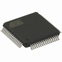
AT90CAN64-16AUR Atmel, AT90CAN64-16AUR Datasheet - Page 350

AT90CAN64-16AUR
Manufacturer Part Number
AT90CAN64-16AUR
Description
MCU AVR 64K FLASH 16MHZ 64TQFP
Manufacturer
Atmel
Series
AVR® 90CANr
Datasheet
1.AT90CAN32-16AUR.pdf
(428 pages)
Specifications of AT90CAN64-16AUR
Core Processor
AVR
Core Size
8-Bit
Speed
16MHz
Connectivity
CAN, EBI/EMI, I²C, SPI, UART/USART
Peripherals
Brown-out Detect/Reset, POR, PWM, WDT
Number Of I /o
53
Program Memory Size
64KB (64K x 8)
Program Memory Type
FLASH
Eeprom Size
2K x 8
Ram Size
4K x 8
Voltage - Supply (vcc/vdd)
2.7 V ~ 5.5 V
Data Converters
A/D 8x10b
Oscillator Type
Internal
Operating Temperature
-40°C ~ 85°C
Package / Case
64-TQFP, 64-VQFP
Data Bus Width
8 bit
Data Ram Size
4 KB
Mounting Style
SMD/SMT
Lead Free Status / RoHS Status
Lead free / RoHS Compliant
Available stocks
Company
Part Number
Manufacturer
Quantity
Price
- Current page: 350 of 428
- Download datasheet (6Mb)
25.8.1
25.8.2
350
AT90CAN32/64/128
Data Polling Flash
Data Polling EEPROM
When a page is being programmed into the Flash, reading an address location within the page
being programmed will give the value 0xFF. At the time the device is ready for a new page, the
programmed value will read correctly. This is used to determine when the next page can be writ-
ten. Note that the entire page is written simultaneously and any address within the page can be
used for polling. Data polling of the Flash will not work for the value 0xFF, so when programming
this value, the user will have to wait for at least t
a chip-erased device contains 0xFF in all locations, programming of addresses that are meant to
contain 0xFF, can be skipped. See
When a new byte has been written and is being programmed into EEPROM, reading the
address location being programmed will give the value 0xFF. At the time the device is ready for
a new byte, the programmed value will read correctly. This is used to determine when the next
byte can be written. This will not work for the value 0xFF, but the user should have the following
in mind: As a chip-erased device contains 0xFF in all locations, programming of addresses that
1. Power-up sequence:
2. Wait for at least 20 ms and enable serial programming by sending the Programming
3. The serial programming instructions will not work if the communication is out of syn-
4. The Flash is programmed one page at a time. The page size is found in
5. The EEPROM array is programmed one byte at a time by supplying the address and
6. Any memory location can be verified by using the Read instruction which returns the
7. At the end of the programming session, RESET can be set high to commence normal
8. Power-off sequence (if needed):
Apply power between V
tems, the programmer can not guarantee that SCK is held low during power-up. In this
case, RESET must be given a positive pulse of at least two CPU clock cycles duration
after SCK has been set to “0”.
Enable serial instruction to pin MOSI.
chronization. When in sync. the second byte (0x53), will echo back when issuing the
third byte of the Programming Enable instruction. Whether the echo is correct or not, all
four bytes of the instruction must be transmitted. If the 0x53 did not echo back, give
RESET a positive pulse and issue a new Programming Enable command.
page
address and data together with the Load Program Memory Page instruction. To ensure
correct loading of the page, the data low byte must be loaded before data high byte is
applied for given address. The Program Memory Page is stored by loading the Write
Program Memory Page instruction with the 9 MSB of the address. If polling is not used,
the user must wait at least t
Note:
data together with the appropriate Write instruction. An EEPROM memory location is
first automatically erased before new data is written. If polling is not used, the user must
wait at least t
erased device, no 0xFFs in the data file(s) need to be programmed.
content at the selected address at serial output MISO.
operation.
Set
Turn Vcc power off.
RESET
341. The memory page is loaded one byte at a time by supplying the 7 LSB of the
EEPROM, Lock bits, Fuses) is completed, may result in incorrect programming. A delay of
1 µs is sufficient.
If other commands than polling (read) are applied before any write operation (Flash,
to “1”.
WD_EEPROM
CC
before issuing the next byte. (See
and GND while RESET and SCK are set to “0”. In some sys-
WD_FLASH
Table 25-14
before issuing the next page. (See
WD_FLASH
for t
WD_FLASH
before programming the next page. As
value.
Table
25-14.) In a chip
Table 25-11 on
Table
7679H–CAN–08/08
25-14).
Related parts for AT90CAN64-16AUR
Image
Part Number
Description
Manufacturer
Datasheet
Request
R

Part Number:
Description:
Manufacturer:
Atmel Corporation
Datasheet:

Part Number:
Description:
Manufacturer:
Atmel Corporation
Datasheet:

Part Number:
Description:
IC MCU AVR 64K FLASH 64-TQFP
Manufacturer:
Atmel
Datasheet:

Part Number:
Description:
IC MCU AVR 64K FLASH 64-QFN
Manufacturer:
Atmel
Datasheet:

Part Number:
Description:
At90can128 8-bit Avr Microcontroller With 32k Bytes Of Isp Flash And Can Controller
Manufacturer:
ATMEL Corporation
Datasheet:

Part Number:
Description:
8-bit Microcontrollers - MCU 64 KB FLASH - 16MHz
Manufacturer:
Atmel

Part Number:
Description:
8-bit Microcontrollers - MCU Microcontroller
Manufacturer:
Atmel

Part Number:
Description:
DEV KIT FOR AVR/AVR32
Manufacturer:
Atmel
Datasheet:


