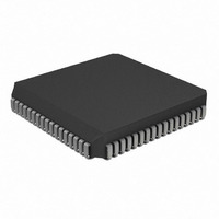
PIC16LC924-04I/L Microchip Technology, PIC16LC924-04I/L Datasheet - Page 38

PIC16LC924-04I/L
Manufacturer Part Number
PIC16LC924-04I/L
Description
IC MCU OTP 4KX14 LCD DVR 68PLCC
Manufacturer
Microchip Technology
Series
PIC® 16Cr
Specifications of PIC16LC924-04I/L
Core Processor
PIC
Core Size
8-Bit
Speed
4MHz
Connectivity
I²C, SPI
Peripherals
LCD, POR, PWM, WDT
Number Of I /o
25
Program Memory Size
7KB (4K x 14)
Program Memory Type
OTP
Ram Size
176 x 8
Voltage - Supply (vcc/vdd)
2.5 V ~ 6 V
Data Converters
A/D 5x8b
Oscillator Type
External
Operating Temperature
-40°C ~ 85°C
Package / Case
68-PLCC
Core
PIC
Processor Series
PIC16LC
Data Bus Width
8 bit
Maximum Clock Frequency
8 MHz
Data Ram Size
176 B
Data Rom Size
176 B
On-chip Adc
8 bit, 5 Channel
Number Of Programmable I/os
25
Number Of Timers
3
Operating Supply Voltage
2.5 V to 6 V
Mounting Style
SMD/SMT
Height
4.06 mm
Interface Type
I2C, SPI
Length
24.33 mm
Maximum Operating Temperature
+ 85 C
Minimum Operating Temperature
- 40 C
Supply Voltage (max)
6 V
Supply Voltage (min)
2.5 V
Width
24.33 mm
Lead Free Status / RoHS Status
Lead free / RoHS Compliant
Eeprom Size
-
Lead Free Status / Rohs Status
Details
Available stocks
Company
Part Number
Manufacturer
Quantity
Price
Company:
Part Number:
PIC16LC924-04I/L
Manufacturer:
Microchip Technology
Quantity:
10 000
PIC16C9XX
5.5
PORTE is an digital input only port. Each pin is multi-
plexed with an LCD segment driver. These pins have
Schmitt Trigger input buffers.
EXAMPLE 5-5:
TABLE 5-9: PORTE FUNCTIONS
TABLE 5-10: SUMMARY OF REGISTERS ASSOCIATED WITH PORTE
DS30444E - page 38
Name
RE0/SEG05
Address Name
09h
89h
10Dh
Legend: Shaded cells are not used by PORTE.
RE1/SEG06
RE2/SEG07
RE3/SEG08
RE4/SEG09
RE5/SEG10
RE6/SEG11
RE7/SEG27
Legend: ST = Schmitt Trigger input
BCF STATUS,RP0
BSF STATUS,RP1
BCF LCDSE,SE27
BCF LCDSE,SE5
BCF LCDSE,SE9
Note 1: On a Power-on Reset these pins are con-
Note 2: To configure the pins as a digital port, the
PORTE and TRISE Register
PORTE
TRISE
LCDSE
figured as LCD segment drivers.
corresponding bits in the LCDSE register
must be cleared. Any bit set in the LCDSE
register overrides any bit settings in the
corresponding TRIS register.
INITIALIZING PORTE
PORTE Data Direction Control Register
Bit#
bit0
bit1
bit2
bit3
bit4
bit5
bit6
bit7
SE29
Bit 7
RE7
;Select Bank2
;
;Make all PORTE
;and PORTG<7>
;digital inputs
Buffer Type
SE27
Bit 6
RE6
ST
ST
ST
ST
ST
ST
ST
ST
SE20
Bit 5
RE5
Digital input or Segment Driver05
Digital input or Segment Driver06
Digital input or Segment Driver07
Digital input or Segment Driver08
Digital input or Segment Driver09
Digital input or Segment Driver10
Digital input or Segment Driver11
Digital input or Segment Driver27 (not available on 64-pin devices)
SE16
Bit 4
RE4
SE12
Bit 3
RE3
FIGURE 5-8: PORTE BLOCK DIAGRAM
Data Bus
RD PORT
RD TRIS
Bit 2
RE2
SE9
LCD Common
Output Enable
LCD Segment
Output Enable
LCD
Common Data
LCDSE<n>
LCD
Segment Data
Bit 1
RE1
SE5
Function
Bit 0
RE0
SE0
V
DD
Q
1997 Microchip Technology Inc.
EN
0000 0000
1111 1111
1111 1111
Power-on
Value on
EN
D
Reset
Digital Input/
LCD Output pin
Schmitt
Trigger
input
buffer
other resets
Value on all
0000 0000
1111 1111
1111 1111


