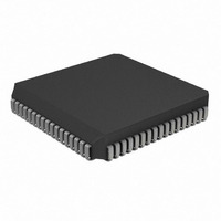
PIC16LC924-04I/L Microchip Technology, PIC16LC924-04I/L Datasheet - Page 76

PIC16LC924-04I/L
Manufacturer Part Number
PIC16LC924-04I/L
Description
IC MCU OTP 4KX14 LCD DVR 68PLCC
Manufacturer
Microchip Technology
Series
PIC® 16Cr
Specifications of PIC16LC924-04I/L
Core Processor
PIC
Core Size
8-Bit
Speed
4MHz
Connectivity
I²C, SPI
Peripherals
LCD, POR, PWM, WDT
Number Of I /o
25
Program Memory Size
7KB (4K x 14)
Program Memory Type
OTP
Ram Size
176 x 8
Voltage - Supply (vcc/vdd)
2.5 V ~ 6 V
Data Converters
A/D 5x8b
Oscillator Type
External
Operating Temperature
-40°C ~ 85°C
Package / Case
68-PLCC
Core
PIC
Processor Series
PIC16LC
Data Bus Width
8 bit
Maximum Clock Frequency
8 MHz
Data Ram Size
176 B
Data Rom Size
176 B
On-chip Adc
8 bit, 5 Channel
Number Of Programmable I/os
25
Number Of Timers
3
Operating Supply Voltage
2.5 V to 6 V
Mounting Style
SMD/SMT
Height
4.06 mm
Interface Type
I2C, SPI
Length
24.33 mm
Maximum Operating Temperature
+ 85 C
Minimum Operating Temperature
- 40 C
Supply Voltage (max)
6 V
Supply Voltage (min)
2.5 V
Width
24.33 mm
Lead Free Status / RoHS Status
Lead free / RoHS Compliant
Eeprom Size
-
Lead Free Status / Rohs Status
Details
Available stocks
Company
Part Number
Manufacturer
Quantity
Price
Company:
Part Number:
PIC16LC924-04I/L
Manufacturer:
Microchip Technology
Quantity:
10 000
PIC16C9XX
11.3.1.3
When the R/W bit of the incoming address byte is set
and an address match occurs, the R/W bit of the
SSPSTAT register is set. The received address is
loaded into the SSPBUF register. The ACK pulse will be
sent on the ninth bit, and pin RC3/SCK/SCL is held low.
The transmit data must be loaded into the SSPBUF
register, which also loads the SSPSR register. Then pin
RC3/SCK/SCL should be enabled by setting bit CKP
(SSPCON<4>). The master must monitor the SCL pin
prior to asserting another clock pulse. The slave
devices may be holding off the master by stretching the
clock. The eight data bits are shifted out on the falling
edge of the SCL input. This ensures that the SDA signal
is valid during the SCL high time (Figure 11-20).
FIGURE 11-20: I
DS30444E - page 76
SDA
SCL
SSPIF (PIR1<3>)
BF (SSPSTAT<0>)
CKP (SSPCON<4>)
S
TRANSMISSION
A7
1
Data in
sampled
2
C WAVEFORMS FOR TRANSMISSION (7-BIT ADDRESS)
A6
2
A5
Receiving Address
3
A4
4
A3
5
A2
6
A1
7
R/W = 1
8
9
ACK
responds to SSPIF
SCL held low
while CPU
An SSP interrupt is generated for each data transfer
byte. Flag bit SSPIF must be cleared in software, and
the SSPSTAT register is used to determine the status of
the byte. Flag bit SSPIF is set on the falling edge of the
ninth clock pulse.
As a slave-transmitter, the ACK pulse from the mas-
ter-receiver is latched on the rising edge of the ninth
SCL input pulse. If the SDA line was high (not ACK),
then the data transfer is complete. When the ACK is
latched by the slave, the slave logic is reset and the
slave then monitors for another occurrence of the
START bit. If the SDA line was low (ACK), the transmit
data must be loaded into the SSPBUF register, which
also
RC3/SCK/SCL should be enabled by setting bit CKP.
D7
1
SSPBUF is written in software
loads
D6
2
Set bit after writing to SSPBUF
(the SSPBUF must be written-to
before the CKP bit can be set)
cleared in software
D5
3
the
D4
4
SSPSR
Transmitting Data
D3
5
1997 Microchip Technology Inc.
D2
6
From SSP interrupt
service routine
D1
7
register.
D0
8
ACK
9
Then
P
pin


