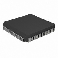
PIC16LC924-04I/L Microchip Technology, PIC16LC924-04I/L Datasheet - Page 63

PIC16LC924-04I/L
Manufacturer Part Number
PIC16LC924-04I/L
Description
IC MCU OTP 4KX14 LCD DVR 68PLCC
Manufacturer
Microchip Technology
Series
PIC® 16Cr
Specifications of PIC16LC924-04I/L
Core Processor
PIC
Core Size
8-Bit
Speed
4MHz
Connectivity
I²C, SPI
Peripherals
LCD, POR, PWM, WDT
Number Of I /o
25
Program Memory Size
7KB (4K x 14)
Program Memory Type
OTP
Ram Size
176 x 8
Voltage - Supply (vcc/vdd)
2.5 V ~ 6 V
Data Converters
A/D 5x8b
Oscillator Type
External
Operating Temperature
-40°C ~ 85°C
Package / Case
68-PLCC
Core
PIC
Processor Series
PIC16LC
Data Bus Width
8 bit
Maximum Clock Frequency
8 MHz
Data Ram Size
176 B
Data Rom Size
176 B
On-chip Adc
8 bit, 5 Channel
Number Of Programmable I/os
25
Number Of Timers
3
Operating Supply Voltage
2.5 V to 6 V
Mounting Style
SMD/SMT
Height
4.06 mm
Interface Type
I2C, SPI
Length
24.33 mm
Maximum Operating Temperature
+ 85 C
Minimum Operating Temperature
- 40 C
Supply Voltage (max)
6 V
Supply Voltage (min)
2.5 V
Width
24.33 mm
Lead Free Status / RoHS Status
Lead free / RoHS Compliant
Eeprom Size
-
Lead Free Status / Rohs Status
Details
Available stocks
Company
Part Number
Manufacturer
Quantity
Price
Company:
Part Number:
PIC16LC924-04I/L
Manufacturer:
Microchip Technology
Quantity:
10 000
11.0
The Synchronous Serial Port (SSP) module is a serial
interface useful for communicating with other periph-
eral or microcontroller devices. These peripheral
devices may be serial EEPROMs, shift registers, dis-
FIGURE 11-1: SSPSTAT: SYNC SERIAL PORT STATUS REGISTER (ADDRESS 94h)
1997 Microchip Technology Inc.
bit7
bit 7:
bit 6:
bit 5:
bit 4:
bit 3:
bit 2:
bit 1:
bit 0:
R/W-0 R/W-0
SMP
SYNCHRONOUS SERIAL
PORT (SSP) MODULE
SMP: SPI data input sample phase
SPI Master Mode
1 = Input data sampled at end of data output time
0 = Input data sampled at middle of data output time
SPI Slave Mode
SMP must be cleared when SPI is used in slave mode
CKE: SPI Clock Edge Select (Figure 11-5, Figure 11-6, and Figure 11-7)
CKP = 0
1 = Data transmitted on rising edge of SCK
0 = Data transmitted on falling edge of SCK
CKP = 1
1 = Data transmitted on falling edge of SCK
0 = Data transmitted on rising edge of SCK
D/A: Data/Address bit (I
1 = Indicates that the last byte received or transmitted was data
0 = Indicates that the last byte received or transmitted was address
P: Stop bit (I
1 = Indicates that a stop bit has been detected last (this bit is '0' on RESET)
0 = Stop bit was not detected last
S: Start bit (I
1 = Indicates that a start bit has been detected last (this bit is '0' on RESET)
0 = Start bit was not detected last
R/W: Read/Write bit information (I
This bit holds the R/W bit information following the last address match. This bit is only valid from the
address match to the next start bit, stop bit, or ACK bit.
1 = Read
0 = Write
UA: Update Address (10-bit I
1 = Indicates that the user needs to update the address in the SSPADD register
0 = Address does not need to be updated
BF: Buffer Full Status bit
Receive (SPI and I
1 = Receive complete, SSPBUF is full
0 = Receive not complete, SSPBUF is empty
Transmit (I
1 = Transmit in progress, SSPBUF is full
0 = Transmit complete, SSPBUF is empty
CKE
detected last)
detected last)
R-0
D/A
2
C mode only)
2
2
C mode only. This bit is cleared when the SSP module is disabled, or when the Start bit was
C mode only. This bit is cleared when the SSP module is disabled, or when the Stop bit was
2
R-0
C modes)
P
2
C mode only)
2
C mode only)
R-0
S
2
C mode only)
R/W
R-0
play drivers, A/D converters, etc. The SSP module can
operate in one of two modes:
• Serial Peripheral Interface (SPI)
• Inter-Integrated Circuit (I
Refer to Application Note AN578, "Use of the SSP
Module in the I
R-0
UA
R-0
BF
2
bit0
C Multi-Master Environment."
R = Readable bit
W = Writable bit
U = Unimplemented bit,
- n =Value at POR reset
PIC16C9XX
2
C)
read as ‘0’
DS30444E - page 63


