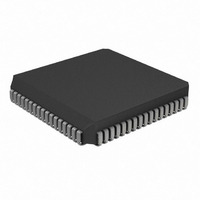
PIC16LC924-04I/L Microchip Technology, PIC16LC924-04I/L Datasheet - Page 84

PIC16LC924-04I/L
Manufacturer Part Number
PIC16LC924-04I/L
Description
IC MCU OTP 4KX14 LCD DVR 68PLCC
Manufacturer
Microchip Technology
Series
PIC® 16Cr
Specifications of PIC16LC924-04I/L
Core Processor
PIC
Core Size
8-Bit
Speed
4MHz
Connectivity
I²C, SPI
Peripherals
LCD, POR, PWM, WDT
Number Of I /o
25
Program Memory Size
7KB (4K x 14)
Program Memory Type
OTP
Ram Size
176 x 8
Voltage - Supply (vcc/vdd)
2.5 V ~ 6 V
Data Converters
A/D 5x8b
Oscillator Type
External
Operating Temperature
-40°C ~ 85°C
Package / Case
68-PLCC
Core
PIC
Processor Series
PIC16LC
Data Bus Width
8 bit
Maximum Clock Frequency
8 MHz
Data Ram Size
176 B
Data Rom Size
176 B
On-chip Adc
8 bit, 5 Channel
Number Of Programmable I/os
25
Number Of Timers
3
Operating Supply Voltage
2.5 V to 6 V
Mounting Style
SMD/SMT
Height
4.06 mm
Interface Type
I2C, SPI
Length
24.33 mm
Maximum Operating Temperature
+ 85 C
Minimum Operating Temperature
- 40 C
Supply Voltage (max)
6 V
Supply Voltage (min)
2.5 V
Width
24.33 mm
Lead Free Status / RoHS Status
Lead free / RoHS Compliant
Eeprom Size
-
Lead Free Status / Rohs Status
Details
Available stocks
Company
Part Number
Manufacturer
Quantity
Price
Company:
Part Number:
PIC16LC924-04I/L
Manufacturer:
Microchip Technology
Quantity:
10 000
PIC16C9XX
12.4
Example 12-2 show how to perform an A/D conversion.
The RA pins are configured as analog inputs. The ana-
log reference (V
rupt is enabled, and the A/D conversion clock is F
The conversion is performed on the RA0 pin
(channel0).
EXAMPLE 12-2: DOING AN A/D CONVERSION
;
;
;
;
DS30444E - page 84
Note:
Ensure that the required acquisition time for the selected input channel has elapsed.
Then the conversion may be started.
BCF
BSF
CLRF
BSF
BCF
MOVLW
MOVWF
BCF
BSF
BSF
BSF
:
:
A/D Conversions
The GO/DONE bit should NOT be set in
the same instruction that turns on the A/D.
STATUS, RP1
STATUS, RP0
ADCON1
PIE1,
STATUS, RP0
0xC1
ADCON0
PIR1,
INTCON, PEIE
INTCON, GIE
ADCON0, GO
REF
) is the device V
ADIE
ADIF
DD
. The A/D inter-
; Select Bank1
;
; Configure A/D inputs
; Enable A/D interrupts
; Select Bank0
; RC Clock, A/D is on, Channel 0 is selected
;
; Clear A/D interrupt flag bit
; Enable peripheral interrupts
; Enable all interrupts
; Start A/D Conversion
; The ADIF bit will be set and the GO/DONE bit
;
is cleared upon completion of the A/D Conversion.
RC
.
Clearing the GO/DONE bit during a conversion will
abort the current conversion. The ADRES register will
NOT be updated with the partially completed A/D con-
version sample. That is, the ADRES register will con-
tinue to contain the value of the last completed
conversion (or the last value written to the ADRES reg-
ister). After the A/D conversion is aborted, a 2T
is required before the next acquisition is started. After
this 2T
the selected channel.
AD
wait, an acquisition is automatically started on
1997 Microchip Technology Inc.
AD
wait


