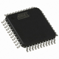
AT89C51CC03CA-RLTUM Atmel, AT89C51CC03CA-RLTUM Datasheet - Page 6

AT89C51CC03CA-RLTUM
Manufacturer Part Number
AT89C51CC03CA-RLTUM
Description
IC 8051 MCU 64K FLASH 44-VQFP
Manufacturer
Atmel
Series
AT89C CANr
Datasheet
1.AT89C51CC03C-S3RIM.pdf
(198 pages)
Specifications of AT89C51CC03CA-RLTUM
Core Processor
8051
Core Size
8-Bit
Speed
40MHz
Connectivity
CAN, UART/USART
Peripherals
POR, PWM, WDT
Number Of I /o
36
Program Memory Size
64KB (64K x 8)
Program Memory Type
FLASH
Eeprom Size
2K x 8
Ram Size
2.25K x 8
Voltage - Supply (vcc/vdd)
3 V ~ 5.5 V
Data Converters
A/D 8x10b
Oscillator Type
External
Operating Temperature
-40°C ~ 85°C
Package / Case
44-TQFP, 44-VQFP
Processor Series
AT89x
Core
8051
Data Bus Width
8 bit
Data Ram Size
2304 B
Interface Type
UART, SPI
Maximum Clock Frequency
60 MHz
Number Of Programmable I/os
36
Number Of Timers
2
Operating Supply Voltage
3 V to 5.5 V
Maximum Operating Temperature
+ 85 C
Mounting Style
SMD/SMT
3rd Party Development Tools
PK51, CA51, A51, ULINK2
Minimum Operating Temperature
- 40 C
On-chip Adc
10 bit, 8 Channel
Package
44VQFP
Device Core
8051
Family Name
AT89
Maximum Speed
60 MHz
For Use With
AT89OCD-01 - USB EMULATOR FOR AT8XC51 MCU
Lead Free Status / RoHS Status
Lead free / RoHS Compliant
Available stocks
Company
Part Number
Manufacturer
Quantity
Price
Company:
Part Number:
AT89C51CC03CA-RLTUM
Manufacturer:
ADI
Quantity:
141
6
Pin Name
P3.0:7
P4.0:4
AT89C51CC03
Type
I/O
I/O
Description
Port 3:
Is an 8-bit bi-directional I/O port with internal pull-ups. Port 3 pins that have 1’s written to them are pulled high by the internal
pull-up transistors and can be used as inputs in this state. As inputs, Port 3 pins that are being pulled low externally will be a
source of current (I
The output latch corresponding to a secondary function must be programmed to one for that function to operate (except for
TxD and WR). The secondary functions are assigned to the pins of port 3 as follows:
P3.0/RxD:
Receiver data input (asynchronous) or data input/output (synchronous) of the serial interface
P3.1/TxD:
Transmitter data output (asynchronous) or clock output (synchronous) of the serial interface
P3.2/INT0:
External interrupt 0 input/timer 0 gate control input
P3.3/INT1:
External interrupt 1 input/timer 1 gate control input
P3.4/T0:
Timer 0 counter input
P3.5/T1/SS:
Timer 1 counter input
SPI Slave Select
P3.6/WR:
External Data Memory write strobe; latches the data byte from port 0 into the external data memory
P3.7/RD:
External Data Memory read strobe; Enables the external data memory.
It can drive CMOS inputs without external pull-ups.
Port 4:
Is an 2-bit bi-directional I/O port with internal pull-ups. Port 4 pins that have 1’s written to them are pulled high by the internal
pull-ups and can be used as inputs in this state. As inputs, Port 4 pins that are being pulled low externally will be a source of
current (IIL, on the datasheet) because of the internal pull-up transistor.
The output latch corresponding to a secondary function RxDC must be programmed to one for that function to operate. The
secondary functions are assigned to the two pins of port 4 as follows:
P4.0/TxDC:
Transmitter output of CAN controller
P4.1/RxDC:
Receiver input of CAN controller.
P4.2/MISO:
Master Input Slave Output of SPI controller
P4.3/SCK:
Serial Clock of SPI controller
P4.4/MOSI:
Master Ouput Slave Input of SPI controller
It can drive CMOS inputs without external pull-ups.
IL
, see section "Electrical Characteristic") because of the internal pull-ups.
4182O–CAN–09/08


