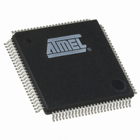
AT91SAM7X512-AU Atmel, AT91SAM7X512-AU Datasheet - Page 19

AT91SAM7X512-AU
Manufacturer Part Number
AT91SAM7X512-AU
Description
MCU ARM 512K HS FLASH 100-LQFP
Manufacturer
Atmel
Series
AT91SAMr
Datasheet
1.AT91SAM7X512-AU-999.pdf
(687 pages)
Specifications of AT91SAM7X512-AU
Core Processor
ARM7
Core Size
16/32-Bit
Speed
55MHz
Connectivity
CAN, Ethernet, I²C, SPI, SSC, UART/USART, USB
Peripherals
Brown-out Detect/Reset, DMA, POR, PWM, WDT
Number Of I /o
62
Program Memory Size
512KB (512K x 8)
Program Memory Type
FLASH
Ram Size
128K x 8
Voltage - Supply (vcc/vdd)
1.65 V ~ 1.95 V
Data Converters
A/D 8x10b
Oscillator Type
Internal
Operating Temperature
-40°C ~ 85°C
Package / Case
100-LQFP
Processor Series
AT91SAMx
Core
ARM7TDMI
Data Bus Width
32 bit
Data Ram Size
128 KB
Interface Type
CAN, SPI, SSC, TWI, USART, USB
Maximum Clock Frequency
55 MHz
Number Of Programmable I/os
13
Number Of Timers
3
Operating Supply Voltage
3 V to 3.6 V
Maximum Operating Temperature
+ 85 C
Mounting Style
SMD/SMT
3rd Party Development Tools
JTRACE-ARM-2M, KSK-AT91SAM7X-PL, MDK-ARM, RL-ARM, ULINK2
Development Tools By Supplier
AT91SAM-ICE, AT91-ISP, AT91SAM7X-EK
Minimum Operating Temperature
- 40 C
On-chip Adc
10 bit
No. Of I/o's
62
Ram Memory Size
128KB
Cpu Speed
55MHz
No. Of Timers
3
No. Of Pwm Channels
4
Digital Ic Case Style
LQFP
Rohs Compliant
Yes
For Use With
AT91SAM-ICE - EMULATOR FOR AT91 ARM7/ARM9AT91SAM7X-EK - KIT EVAL FOR AT91SAM7X256/128
Lead Free Status / RoHS Status
Lead free / RoHS Compliant
Eeprom Size
-
Lead Free Status / Rohs Status
Lead free / RoHS Compliant
Available stocks
Company
Part Number
Manufacturer
Quantity
Price
Company:
Part Number:
AT91SAM7X512-AU
Manufacturer:
Atmel
Quantity:
10 000
Company:
Part Number:
AT91SAM7X512-AU
Manufacturer:
ATMEL
Quantity:
717
- Current page: 19 of 687
- Download datasheet (11Mb)
8.4
8.4.1
8.4.2
8.4.3
6120H–ATARM–17-Feb-09
Memory Mapping
Internal SRAM
Internal ROM
Internal Flash
After reset and until the Remap Command is performed, the SRAM is only accessible at address
0x0020 0000. After Remap, the SRAM also becomes available at address 0x0.
The AT91SAM7X512/256/128 embeds an Internal ROM. At any time, the ROM is mapped at
address 0x30 0000. The ROM contains the FFPI and the SAM-BA program.
At any time, the Flash is mapped to address 0x0010 0000. It is also accessible at address 0x0
after the reset, if GPNVM bit 2 is set and before the Remap Command.
A general purpose NVM (GPNVM) bit is used to boot either on the ROM (default) or from the
Flash.
This GPNVM bit can be cleared or set respectively through the commands “Clear General-pur-
pose NVM Bit” and “Set General-purpose NVM Bit” of the EFC User Interface.
Setting the GPNVM Bit 2 selects the boot from the Flash. Asserting ERASE clears the GPNVM
Bit 2 and thus selects the boot from the ROM by default.
Figure 8-2.
• The AT91SAM7X512 embeds a high-speed 128 Kbyte SRAM bank.
• The AT91SAM7X256 embeds a high-speed 64 Kbyte SRAM bank.
• The AT91SAM7X128 embeds a high-speed 32 Kbyte SRAM bank.
• The AT91SAM7X512 features two banks (dual plane) of 256 Kbytes of Flash.
• The AT91SAM7X256 features one bank (single plane) of 256 Kbytes of Flash.
• The AT91SAM7X128 features one bank (single plane) of 128 Kbytes of Flash.
256M Bytes
Internal Memory Mapping with GPNVM Bit 2 = 0 (default)
0x0000 0000
0x0010 0000
0x0020 0000
0x0030 0000
0x000F FFFF
0x001F FFFF
0x002F FFFF
0x0FFF FFFF
0x003F FFFF
0x0040 0000
AT91SAM7X512/256/128 Preliminary
ROM Before Remap
SRAM After Remap
Undefined Areas
Internal FLASH
Internal SRAM
Internal ROM
(Abort)
252 M Bytes
1 M Bytes
1 M Bytes
1 M Bytes
1 M Bytes
19
Related parts for AT91SAM7X512-AU
Image
Part Number
Description
Manufacturer
Datasheet
Request
R

Part Number:
Description:
KIT EVAL FOR AT91SAM7X256/128
Manufacturer:
Atmel
Datasheet:

Part Number:
Description:
MCU, MPU & DSP Development Tools KICKSTART KIT ATMEL AT91SAM7X
Manufacturer:
IAR Systems

Part Number:
Description:
DEV KIT FOR AVR/AVR32
Manufacturer:
Atmel
Datasheet:

Part Number:
Description:
INTERVAL AND WIPE/WASH WIPER CONTROL IC WITH DELAY
Manufacturer:
ATMEL Corporation
Datasheet:

Part Number:
Description:
Low-Voltage Voice-Switched IC for Hands-Free Operation
Manufacturer:
ATMEL Corporation
Datasheet:

Part Number:
Description:
MONOLITHIC INTEGRATED FEATUREPHONE CIRCUIT
Manufacturer:
ATMEL Corporation
Datasheet:

Part Number:
Description:
AM-FM Receiver IC U4255BM-M
Manufacturer:
ATMEL Corporation
Datasheet:

Part Number:
Description:
Monolithic Integrated Feature Phone Circuit
Manufacturer:
ATMEL Corporation
Datasheet:

Part Number:
Description:
Multistandard Video-IF and Quasi Parallel Sound Processing
Manufacturer:
ATMEL Corporation
Datasheet:

Part Number:
Description:
High-performance EE PLD
Manufacturer:
ATMEL Corporation
Datasheet:

Part Number:
Description:
8-bit Flash Microcontroller
Manufacturer:
ATMEL Corporation
Datasheet:

Part Number:
Description:
2-Wire Serial EEPROM
Manufacturer:
ATMEL Corporation
Datasheet:


