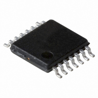
P87LPC760BDH,112 NXP Semiconductors, P87LPC760BDH,112 Datasheet - Page 8

P87LPC760BDH,112
Manufacturer Part Number
P87LPC760BDH,112
Description
IC 80C51 MCU 1K OTP 14-TSSOP
Manufacturer
NXP Semiconductors
Series
LPC700r
Datasheet
1.P87LPC760BN112.pdf
(56 pages)
Specifications of P87LPC760BDH,112
Program Memory Type
OTP
Program Memory Size
1KB (1K x 8)
Package / Case
14-TSSOP
Core Processor
8051
Core Size
8-Bit
Speed
20MHz
Connectivity
I²C, UART/USART
Peripherals
Brown-out Detect/Reset, LED, POR, WDT
Number Of I /o
12
Ram Size
128 x 8
Voltage - Supply (vcc/vdd)
2.7 V ~ 6 V
Oscillator Type
Internal
Operating Temperature
0°C ~ 70°C
Processor Series
P87LPC7x
Core
80C51
Data Bus Width
8 bit
Data Ram Size
128 B
Interface Type
I2C/UART
Maximum Clock Frequency
20 MHz
Number Of Programmable I/os
12
Number Of Timers
2
Operating Supply Voltage
2.7 V to 6 V
Maximum Operating Temperature
+ 70 C
Mounting Style
SMD/SMT
3rd Party Development Tools
PK51, CA51, A51, ULINK2
Minimum Operating Temperature
0 C
Lead Free Status / RoHS Status
Lead free / RoHS Compliant
For Use With
OM10063 - PROGRAMMER LPC700 P76XLCPOM10050 - EMULATOR LPC700 PDS76X
Eeprom Size
-
Data Converters
-
Lead Free Status / Rohs Status
Lead free / RoHS Compliant
Other names
568-1015-5
935271146112
P87LPC760BDH
935271146112
P87LPC760BDH
Philips Semiconductors
PIN DESCRIPTIONS
2002 Mar 07
P0.3–P0.6
P1.0–P1.3
P1.5, P1.7
P2.0–P2.1
V
V
Low power, low price, low pin count (14 pin)
microcontroller with 1 kbyte OTP
SS
DD
MNEMONIC
10, 12–14
PIN NO.
1–2
6–9
4, 5
14
13
12
10
11
9
8
7
6
2
5
4
3
TYPE
I/O
I/O
I/O
I/O
I/O
I/O
O
O
O
I
I
I
I
I
I
I
I
I
Port 0: Port 0 is an 4-bit I/O port with a user-configurable output type. Port 0 latches are
configured in the quasi-bidirectional mode and have either ones or zeros written to them
during reset, as determined by the PRHI bit in the UCFG1 configuration byte. The operation
of port 0 pins as inputs and outputs depends upon the port configuration selected. Each port
pin is configured independently. Refer to the section on I/O port configuration and the DC
Electrical Characteristics for details.
The Keyboard Interrupt feature operates with port 0 pins.
Port 0 also provides various special functions as described below.
Port 1: Port 1 is an 6-bit I/O port with a user-configurable output type, except for three pins
as noted below. Port 1 latches are configured in the quasi-bidirectional mode and have ei-
ther ones or zeros written to them during reset, as determined by the PRHI bit in the UCFG1
configuration byte. The operation of the configurable port 1 pins as inputs and outputs de-
pends upon the port configuration selected. Each of the configurable port pins are pro-
grammed independently. Refer to the section on I/O port configuration and the DC Electrical
Characteristics for details.
Port 1 also provides various special functions as described below.
Port 2: Port 2 is a 2-bit I/O port with a user-configurable output type. Port 2 latches are con-
figured in the quasi-bidirectional mode and have either ones or zeros written to them during
reset, as determined by the PRHI bit in the UCFG1 configuration byte. The operation of port
2 pins as inputs and outputs depends upon the port configuration selected. Each port pin is
configured independently. Refer to the section on I/O port configuration and the DC Electri-
cal Characteristics for details.
Port 2 also provides various special functions as described below.
Ground: 0 V reference.
Power Supply: This is the power supply voltage for normal operation as well as Idle and
Power Down modes.
P0.3
P0.4
P0.5
P0.6
P1.0
P1.1
P1.2
P1.3
P1.5
P2.0
P2.1
CIN1B
CIN1A
CMPREF
CMP1
TxD
RxD
T0
SCL
INT0
SDA
RST
X2
CLKOUT
X1
5
Comparator 1 positive input B.
Comparator 1 positive input A
Comparator reference (negative) input.
Comparator 1 output
Transmitter output for the serial port.
Receiver input for the serial port.
Timer/counter 0 external count input or overflow output.
I
P1.2 is open drain, in order to conform to I
External interrupt 0 input.
I
is open drain, in order to conform to I
External Reset input (if selected via EPROM configuration). A
low on this pin resets the microcontroller, causing I/O ports and
peripherals to take on their default states, and the processor
begins execution at address 0. When used as a port pin, P1.5 is
a Schmitt trigger input only.
Output from the oscillator amplifier (when a crystal oscillator
option is selected via the EPROM configuration).
CPU clock divided by 6 clock output when enabled via SFR bit
and in conjunction with internal RC oscillator or external clock
input.
Input to the oscillator circuit and internal clock generator circuits
(when selected via the EPROM configuration).
2
2
C serial clock input/output. When configured as an output,
C serial data input/output. When configured as an output, P1.3
NAME AND FUNCTION
2
C specifications.
P87LPC760
2
C specifications.
Preliminary data


