P89LPC9321FA,529 NXP Semiconductors, P89LPC9321FA,529 Datasheet
P89LPC9321FA,529
Specifications of P89LPC9321FA,529
Available stocks


Related parts for P89LPC9321FA,529


P89LPC9321FA,529 Summary of contents
Page 1
P89LPC9321 8-bit microcontroller with accelerated two-clock 80C51 core byte-erasable flash with 512-byte data EEPROM Rev. 2 — 16 November 2010 1. General description The P89LPC9321 is a single-chip microcontroller, available in low cost packages, based on ...
Page 2
... NXP Semiconductors 2.2 Additional features A high performance 80C51 CPU provides instruction cycle times of 111 ns to 222 ns for all instructions except multiply and divide when executing at 18 MHz. This is six times the performance of the standard 80C51 running at the same clock frequency. A lower clock frequency for the same performance results in power savings and reduced EMI ...
Page 3
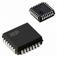
... NXP Semiconductors 3. Ordering information Table 1. Type number P89LPC9321FA P89LPC9321FDH P89LPC9321FN 3.1 Ordering options Table 2. Type number P89LPC9321FA P89LPC9321FDH P89LPC9321FN P89LPC9321 Product data sheet 8-bit microcontroller with accelerated two-clock 80C51 core Ordering information Package Name Description PLCC28 plastic leaded chip carrier; 28 leads TSSOP28 plastic thin shrink small outline package ...
Page 4
... NXP Semiconductors 4. Block diagram P89LPC9321 P3[1:0] P2[7:0] P1[7:0] P0[7:0] XTAL1 CRYSTAL OR RESONATOR XTAL2 Fig 1. Block diagram P89LPC9321 Product data sheet 8-bit microcontroller with accelerated two-clock 80C51 core ACCELERATED 2-CLOCK 80C51 CPU 8 kB CODE FLASH internal bus 256-BYTE DATA RAM 512-BYTE AUXILIARY RAM ...
Page 5
... NXP Semiconductors 5. Functional diagram KBI0 KBI1 KBI2 KBI3 KBI4 KBI5 KBI6 KBI7 CLKOUT Fig 2. Functional diagram P89LPC9321 Product data sheet 8-bit microcontroller with accelerated two-clock 80C51 core CMP2 CIN2B CIN2A CIN1B PORT 0 CIN1A CMPREF CMP1 T1 P89LPC9321 XTAL2 PORT 3 XTAL1 002aae103 All information provided in this document is subject to legal disclaimers. ...
Page 6
... NXP Semiconductors 6. Pinning information 6.1 Pinning Fig 3. Fig 4. P89LPC9321 Product data sheet 8-bit microcontroller with accelerated two-clock 80C51 core P2.0/ICB 1 2 P2.1/OCD 3 P0.0/CMP2/KBI0 P1.7/OCC 4 P1.6/OCB 5 P1.5/RST P89LPC9321FDH 8 P3.1/XTAL1 P3.0/XTAL2/CLKOUT 9 P1.4/INT1 10 P1.3/INT0/SDA 11 12 P1.2/T0/SCL 13 P2.2/MOSI 14 P2.3/MISO P89LPC9321 TSSOP28 pin configuration P1.6/OCB 5 6 P1.5/RST ...
Page 7
... NXP Semiconductors Fig 5. P89LPC9321 Product data sheet 8-bit microcontroller with accelerated two-clock 80C51 core P2.0/ICB 1 2 P2.1/OCD 3 P0.0/CMP2/KBI0 P1.7/OCC 4 P1.6/OCB 5 P1.5/RST P89LPC9321FN 8 P3.1/XTAL1 9 P3.0/XTAL2/CLKOUT P1.4/INT1 10 P1.3/INT0/SDA 11 12 P1.2/T0/SCL 13 P2.2/MOSI 14 P2.3/MISO P89LPC9321 DIP28 pin configuration All information provided in this document is subject to legal disclaimers. ...
Page 8
... NXP Semiconductors 6.2 Pin description Table 3. Pin description Symbol Pin P0.0 to P0.7 P0.0/CMP2/ 3 KBI0 P0.1/CIN2B/ 26 KBI1 P0.2/CIN2A/ 25 KBI2 P0.3/CIN1B/ 24 KBI3 P0.4/CIN1A/ 23 KBI4 P0.5/CMPREF/ 22 KBI5 P89LPC9321 Product data sheet 8-bit microcontroller with accelerated two-clock 80C51 core Type Description I/O Port 0: Port 8-bit I/O port with a user-configurable output type. During reset Port 0 latches are configured in the input only mode with the internal pull-up disabled ...
Page 9
... NXP Semiconductors Table 3. Pin description …continued Symbol Pin P0.6/CMP1/KBI6 20 P0.7/T1/KBI7 19 P1.0 to P1.7 P1.0/TXD 18 P1.1/RXD 17 P1.2/T0/SCL 12 P1.3/INT0/SDA 11 P1.4/INT1 10 P1.5/RST 6 P1.6/OCB 5 P1.7/OCC 4 P2.0 to P2.7 P89LPC9321 Product data sheet 8-bit microcontroller with accelerated two-clock 80C51 core Type Description I/O P0.6 — Port 0 bit 6. High current source. ...
Page 10
... NXP Semiconductors Table 3. Pin description …continued Symbol Pin P2.0/ICB 1 P2.1/OCD 2 P2.2/MOSI 13 P2.3/MISO 14 P2.4/SS 15 P2.5/SPICLK 16 P2.6/OCA 27 P2.7/ICA 28 P3.0 to P3.1 P3.0/XTAL2/ 9 CLKOUT P3.1/XTAL1 [1] Input/output for P1.0 to P1.4, P1.6, P1.7. Input for P1.5. P89LPC9321 Product data sheet 8-bit microcontroller with accelerated two-clock 80C51 core ...
Page 11
... NXP Semiconductors 7. Functional description Remark: Please refer to the P89LPC9321 User manual for a more detailed functional description. 7.1 Special function registers Remark: SFR accesses are restricted in the following ways: • User must not attempt to access any SFR locations not defined. • Accesses to any defined SFR locations must be strictly for the functions for the SFRs. ...
Page 12
Table 4. Special function registers * indicates SFRs that are bit addressable. Name Description SFR Bit functions and addresses addr. MSB Bit address E7 ACC* Accumulator E0H AUXR1 Auxiliary A2H CLKLP function register Bit address register F0H ...
Page 13
Table 4. Special function registers …continued * indicates SFRs that are bit addressable. Name Description SFR Bit functions and addresses addr. MSB DEEDAT Data EEPROM F2H data register DEEADR Data EEPROM F3H address register DIVM CPU clock 95H divide-by-M control ...
Page 14
Table 4. Special function registers …continued * indicates SFRs that are bit addressable. Name Description SFR Bit functions and addresses addr. MSB I2SCLH Serial clock DDH generator/SCL duty cycle register high I2SCLL Serial clock DCH generator/SCL duty cycle register low ...
Page 15
Table 4. Special function registers …continued * indicates SFRs that are bit addressable. Name Description SFR Bit functions and addresses addr. MSB KBCON Keypad control 94H - register KBMASK Keypad 86H interrupt mask register KBPATN Keypad pattern 93H register OCRAH ...
Page 16
Table 4. Special function registers …continued * indicates SFRs that are bit addressable. Name Description SFR Bit functions and addresses addr. MSB P1* Port 1 90H OCC Bit address A7 P2* Port 2 A0H ICA Bit address B7 P3* Port ...
Page 17
Table 4. Special function registers …continued * indicates SFRs that are bit addressable. Name Description SFR Bit functions and addresses addr. MSB RTCH RTC register D2H high RTCL RTC register D3H low SADDR Serial port A9H address register SADEN Serial ...
Page 18
Table 4. Special function registers …continued * indicates SFRs that are bit addressable. Name Description SFR Bit functions and addresses addr. MSB TH0 Timer 0 high 8CH TH1 Timer 1 high 8DH TH2 CCU timer high CDH TICR2 CCU interrupt ...
Page 19
Table 4. Special function registers …continued * indicates SFRs that are bit addressable. Name Description SFR Bit functions and addresses addr. MSB WDL Watchdog load C1H WFEED1 Watchdog C2H feed 1 WFEED2 Watchdog C3H feed 2 [1] All ports are ...
Page 20
Table 5. Extended special function registers Name Description SFR Bit functions and addresses addr. BODCFG BOD FFC8H configuration register CLKCON CLOCK Control FFDEH CLKOK register PGACON1 PGA1 control FFE1H ENPGA1 register PGACON1B PGA1 control FFE4H register B PGA1TRIM8X16X PGA1 trim ...
Page 21
... NXP Semiconductors 7.2 Enhanced CPU The P89LPC9321 uses an enhanced 80C51 CPU which runs at six times the speed of standard 80C51 devices. A machine cycle consists of two CPU clock cycles, and most instructions execute in one or two machine cycles. 7.3 Clocks 7.3.1 Clock definitions The P89LPC9321 device has several internal clocks as defined below: OSCCLK — ...
Page 22
... NXP Semiconductors 7.5 Clock output The P89LPC9321 supports a user-selectable clock output function on the XTAL2/CLKOUT pin when crystal oscillator is not being used. This condition occurs if another clock source has been selected (on-chip RC oscillator, watchdog oscillator, external clock input on XTAL1) and if the RTC and WDT are not using the crystal oscillator as their clock source ...
Page 23
... NXP Semiconductors HIGH FREQUENCY XTAL1 MEDIUM FREQUENCY XTAL2 LOW FREQUENCY RC OSCILLATOR WITH CLOCK DOUBLER (7.3728 MHz/14.7456 MHz ± WATCHDOG OSCILLATOR (400 kHz ± Fig 6. Block diagram of oscillator control 7.10 CCLK wake-up delay The P89LPC9321 has an internal wake-up timer that delays the clock until it stabilizes depending on the clock source used ...
Page 24
... NXP Semiconductors 7.13 Memory organization The various P89LPC9321 memory spaces are as follows: • DATA 128 bytes of internal data memory space (00H:7FH) accessed via direct or indirect addressing, using instructions other than MOVX and MOVC. All or part of the Stack may be in this area. ...
Page 25
... NXP Semiconductors Each interrupt source can be individually programmed to one of four priority levels by setting or clearing bits in the interrupt priority registers IP0, IP0H, IP1 and IP1H. An interrupt service routine in progress can be interrupted by a higher priority interrupt, but not by another interrupt of the same or lower priority. The highest priority interrupt service cannot be interrupted by any other interrupt source ...
Page 26
... NXP Semiconductors RTCF ERTC (RTCCON.1) WDOVF any CCU interrupt Fig 7. Interrupt sources, interrupt enables, and power-down wake-up sources P89LPC9321 Product data sheet 8-bit microcontroller with accelerated two-clock 80C51 core IE0 EX0 IE1 EX1 BOIF EBO KBIF EKBI EWDRT CMF2 CMF1 EC EA (IE0.7) ...
Page 27
... NXP Semiconductors 7.16 I/O ports The P89LPC9321 has four I/O ports: Port 0, Port 1, Port 2 and Port 3. Ports 0, 1, and 2 are 8-bit ports, and Port 2-bit port. The exact number of I/O pins available depends upon the clock and reset options chosen, as shown in Table 7 ...
Page 28
... NXP Semiconductors An open-drain port pin has a Schmitt trigger input that also has a glitch suppression circuit. 7.16.1.3 Input-only configuration The input-only port configuration has no output drivers Schmitt trigger input that also has a glitch suppression circuit. 7.16.1.4 Push-pull output configuration The push-pull output configuration has the same pull-down structure as both the open-drain and the quasi-bidirectional output modes, but provides a continuous strong pull-up when the port latch contains a logic 1 ...
Page 29
... NXP Semiconductors 7.17.1 Brownout detection The brownout detect function determines if the power supply voltage drops below a certain level. Enhanced brownout detection has 3 independent functions: BOD reset, BOD interrupt and BOD EEPROM/FLASH. BOD reset is always on except in total power-down mode. It could not be disabled in software ...
Page 30
... NXP Semiconductors Some chip functions continue to operate and draw power during Power-down mode, increasing the total power used during power-down. These include: Brownout detect, watchdog timer, comparators (note that comparators can be powered down separately), and RTC/system timer. The internal RC oscillator is disabled unless both the RC oscillator has been selected as the system clock and the RTC is enabled ...
Page 31
... NXP Semiconductors 7.19.1 Reset vector Following reset, the P89LPC9321 will fetch instructions from either address 0000H or the Boot address. The Boot address is formed by using the boot vector as the high byte of the address and the low byte of the address = 00H. The boot address will be used if a UART break reset occurs, or the non-volatile boot status bit (BOOTSTAT ...
Page 32
... NXP Semiconductors 7.20.6 Timer overflow toggle output Timers 0 and 1 can be configured to automatically toggle a port output whenever a timer overflow occurs. The same device pins that are used for the T0 and T1 count inputs are also used for the timer toggle outputs. The port outputs will be a logic 1 prior to the first timer overflow when this mode is turned on ...
Page 33
... NXP Semiconductors When a reload occurs, the CCU Timer Overflow Interrupt Flag will be set, and an interrupt generated if enabled. The 16-bit CCU timer may also be used as an 8-bit up/down timer. 7.22.4 Output compare There are four output compare channels and D. Each output compare channel needs to be enabled in order to operate and the user will have to set the associated I/O pin to the desired output mode to connect the pin ...
Page 34
... NXP Semiconductors Fig 9. 7.22.7 Alternating output mode In asymmetrical mode, the user can set up PWM channels A/B and C/D as alternating pairs for bridge drive control. In this mode the output of these PWM channels are alternately gated on every counter cycle. Fig 10. Alternate output mode 7 ...
Page 35
... NXP Semiconductors Since N ranges from 0 to 15, the CCLK frequency can be in the range of PCLK to PCLK16. 7.22.9 CCU interrupts There are seven interrupt sources on the CCU which share a common interrupt vector. EA (IEN0.7) ECCU (IEN1.4) TOIE2 (TICR2.7) TOIF2 (TIFR2.7) TICIE2A (TICR2.0) TICF2A (TIFR2.0) TICIE2B (TICR2 ...
Page 36
... NXP Semiconductors 7.23.2 Mode 1 10 bits are transmitted (through TXD) or received (through RXD): a start bit (logic 0), 8 data bits (LSB first), and a stop bit (logic 1). When data is received, the stop bit is stored in RB8 in special function register SCON. The baud rate is variable and is determined by ...
Page 37
... NXP Semiconductors 7.23.7 Break detect Break detect is reported in the status register (SSTAT). A break is detected when 11 consecutive bits are sensed LOW. The break detect can be used to reset the device and force the device into ISP mode. 7.23.8 Double buffering The UART has a transmit double buffer that allows buffering of the next character to be written to SnBUF while the first character is being transmitted ...
Page 38
... NXP Semiconductors Fig 13. I P89LPC9321 Product data sheet 8-bit microcontroller with accelerated two-clock 80C51 core 2 I C-bus P1.3/SDA P1.2/SCL P89LPC9321 2 C-bus configuration All information provided in this document is subject to legal disclaimers. Rev. 2 — 16 November 2010 P89LPC9321 OTHER DEVICE OTHER DEVICE 2 2 WITH I ...
Page 39
... NXP Semiconductors P1.3/SDA P1.2/SCL Fig 14. I P89LPC9321 Product data sheet 8-bit microcontroller with accelerated two-clock 80C51 core P1.3 INPUT FILTER OUTPUT STAGE INPUT FILTER OUTPUT STAGE timer 1 overflow P1.2 I2CON I2SCLH I2SCLL status bus I2STAT 2 C-bus serial interface block diagram All information provided in this document is subject to legal disclaimers. ...
Page 40
... NXP Semiconductors 7.25 SPI The P89LPC9321 provides another high-speed serial communication interface: the SPI interface. SPI is a full-duplex, high-speed, synchronous communication bus with two operation modes: Master mode and Slave mode Mbit/s can be supported in either Master mode or Slave mode. It has a Transfer Completion Flag and Write Collision Flag Protection ...
Page 41
... NXP Semiconductors 7.25.1 Typical SPI configurations Fig 16. SPI single master single slave configuration Fig 17. SPI dual device configuration, where either can be a master or a slave P89LPC9321 Product data sheet 8-bit microcontroller with accelerated two-clock 80C51 core master MISO 8-BIT SHIFT MOSI ...
Page 42
... NXP Semiconductors Fig 18. SPI single master multiple slaves configuration 7.26 Analog comparators Two analog comparators are provided on the P89LPC9321. Input and output options allow use of the comparators in a number of different configurations. Comparator operation is such that the output is a logical one (which may be read in a register and/or routed to a pin) when the positive input (one of two selectable inputs) is greater than the negative input (selectable from a pin or an internal reference voltage) ...
Page 43
... NXP Semiconductors (P0.4) CIN1A (P0.3) CIN1B PGA1 (P0.5) CMPREF (P0.2) CIN2A (P0.1) CIN2B Fig 19. Comparator input and output connections 7.26.1 Internal reference voltage An internal reference voltage generator may supply a default reference when a single comparator input pin is used. The value of the internal reference voltage, referred 1.23 V ± ...
Page 44
... NXP Semiconductors 7.27 KBI The Keypad Interrupt function (KBI) is intended primarily to allow a single interrupt to be generated when Port 0 is equal to or not equal to a certain pattern. This function can be used for bus address recognition or keypad recognition. The user can configure the port via SFRs for different tasks ...
Page 45
... NXP Semiconductors MOV WFEED1, #0A5H MOV WFEED2, #05AH PCLK 0 0 watchdog 1 crystal oscillator 1 oscillator XTALWD WDCON (A7H) (1) Watchdog reset can also be caused by an invalid feed sequence writing to WDCON not immediately followed by a feed sequence. Fig 20. Watchdog timer in Watchdog mode (WDTE = 1) 7.29 Additional features 7 ...
Page 46
... NXP Semiconductors After the operation finishes, the hardware will set the EEIF bit, which if enabled will generate an interrupt. The flag is cleared by software. Remark: When voltage supply is lower than 2.4 V, the BOD FLASH is tripped and Data EEPROM program or erase is blocked. EWERR1 and EWERR0 bits are used to indicate the write error for BOD EEPROM ...
Page 47
... NXP Semiconductors 7.30.4 Using flash as data storage The flash code memory array of this device supports individual byte erasing and programming. Any byte in the code memory array may be read using the MOVC instruction, provided that the sector containing the byte has not been secured (a MOVC instruction is not allowed to read code memory contents of a secured sector) ...
Page 48
... NXP Semiconductors 7.30.8 ISP ISP is performed without removing the microcontroller from the system. The ISP facility consists of a series of internal hardware resources coupled with internal firmware to facilitate remote programming of the P89LPC9321 through the serial port. This firmware is provided by NXP and embedded within each P89LPC9321 device. The NXP ISP facility has made in-system programming in an embedded application possible with a minimum of additional expense in components and circuit board area ...
Page 49
... NXP Semiconductors 7.32 User sector security bytes There are eight User Sector Security Bytes on the P89LPC9321. Each byte corresponds to one sector. Please see the P89LPC9321 User manual for additional details. 7.33 PGA Additional PGA module is integrated. The gain of PGA can be programmable and 16 ...
Page 50
... NXP Semiconductors 8. Limiting values Table 9. Limiting values In accordance with the Absolute Maximum Rating System (IEC 60134). Symbol Parameter T bias ambient temperature amb(bias) T storage temperature stg I HIGH-level output current per OH(I/O) input/output pin I LOW-level output current per OL(I/O) input/output pin I maximum total input/output current ...
Page 51
... NXP Semiconductors 9. Static characteristics Table 10. Static characteristics 3.6 V unless otherwise specified. DD − ° ° +85 C for industrial applications, unless otherwise specified. amb Symbol Parameter I operating supply current DD(oper) I Idle mode supply current DD(idle) I Power-down mode supply DD(pd) current I total Power-down mode supply ...
Page 52
... NXP Semiconductors Table 10. Static characteristics 3.6 V unless otherwise specified. DD − ° ° +85 C for industrial applications, unless otherwise specified. amb Symbol Parameter I HIGH-LOW transition current THL R internal pull-up resistance on RST_N(int) pin RST BOD interrupt V trip voltage trip BOD reset V trip voltage ...
Page 53
... NXP Semiconductors [5] This specification can be applied to pins which have A/D input or analog comparator input functions when the pin is not being used for those analog functions. When the pin is being used as an analog input pin, the maximum voltage on the pin must be limited to 4.0 V with respect to V ...
Page 54
... NXP Semiconductors 10. Dynamic characteristics Table 11. Dynamic characteristics (12 MHz 2 3.6 V unless otherwise specified. DD − ° ° +85 C for industrial applications, unless otherwise specified. amb Symbol Parameter f internal RC oscillator osc(RC) frequency f internal watchdog osc(WD) oscillator frequency f oscillator frequency osc T clock cycle time cy(clk) ...
Page 55
... NXP Semiconductors Table 11. Dynamic characteristics (12 MHz 2 3.6 V unless otherwise specified. DD − ° ° +85 C for industrial applications, unless otherwise specified. amb Symbol Parameter T SPI cycle time SPICYC slave master t SPI enable lead time SPILEAD slave t SPI enable lag time SPILAG slave ...
Page 56
... NXP Semiconductors Table 12. Dynamic characteristics (18 MHz 3 3.6 V unless otherwise specified. DD − ° ° +85 C for industrial applications, unless otherwise specified. amb Symbol Parameter f internal RC oscillator osc(RC) frequency f internal watchdog osc(WD) oscillator frequency f oscillator frequency osc T clock cycle time cy(clk) f low-power select clock ...
Page 57
... NXP Semiconductors Table 12. Dynamic characteristics (18 MHz 3 3.6 V unless otherwise specified. DD − ° ° +85 C for industrial applications, unless otherwise specified. amb Symbol Parameter t SPI enable lead time SPILEAD slave t SPI enable lag time SPILAG slave t SPICLK HIGH time SPICLKH slave master ...
Page 58
... NXP Semiconductors 10.1 Waveforms clock t QVXH output data write to SBUF t XHDV input data clear RI Fig 21. Shift register mode timing Fig 22. External clock timing SS SPICLK (CPOL = 0) (output) SPICLK (CPOL = 1) (output) MISO (input) t MOSI SPIF (output) Fig 23. SPI master timing (CPHA = 0) P89LPC9321 Product data sheet ...
Page 59
... NXP Semiconductors SS SPICLK (CPOL = 0) (output) SPICLK (CPOL = 1) (output) MISO (input) t SPIF MOSI (output) Fig 24. SPI master timing (CPHA = SPIF t SPILEAD SPICLK (CPOL = 0) (input) t SPICLK (CPOL = 1) (input) t SPIA MISO (output) t SPIDSU MOSI (input) Fig 25. SPI slave timing (CPHA = 0) P89LPC9321 Product data sheet ...
Page 60
... NXP Semiconductors SS t SPIF t SPILEAD SPICLK (CPOL = 0) (input) t SPIF SPICLK (CPOL = 1) (input) t SPIOH t SPIDV t SPIA MISO not defined (output) MOSI (input) Fig 26. SPI slave timing (CPHA = 1) 10.2 ISP entry mode Table 13. Dynamic characteristics, ISP entry mode 3.6 V, unless otherwise specified. ...
Page 61
... NXP Semiconductors 11. Other characteristics 11.1 Comparator electrical characteristics Table 14. Comparator electrical characteristics 3.6 V, unless otherwise specified. DD − ° ° +85 C for industrial applications, unless otherwise specified. amb Symbol Parameter V input offset voltage IO V common-mode input voltage IC CMRR common-mode rejection ratio ...
Page 62
... NXP Semiconductors 11.2 PGA electrical characteristics Table 15. PGA electrical characteristics 3.6 V, unless otherwise specified. DD − ° ° +85 C for industrial applications, unless otherwise specified. amb All limits valid for an external source impedance of less than 10 k Symbol Parameter t PGA settling time ...
Page 63
... NXP Semiconductors 12. Package outline PLCC28: plastic leaded chip carrier; 28 leads pin 1 index 4 β DIMENSIONS (mm dimensions are derived from the original inch dimensions UNIT min. max. 4.57 0.53 mm 0.51 0.25 3.05 4.19 0.33 0.180 0.021 inches 0.02 0.01 0.12 0.165 0.013 Note 1 ...
Page 64
... NXP Semiconductors TSSOP28: plastic thin shrink small outline package; 28 leads; body width 4 pin 1 index 1 DIMENSIONS (mm are the original dimensions) A UNIT max. 0.15 0.95 mm 1.1 0.25 0.05 0.80 Notes 1. Plastic or metal protrusions of 0.15 mm maximum per side are not included. 2. Plastic interlead protrusions of 0.25 mm maximum per side are not included. ...
Page 65
... NXP Semiconductors DIP28: plastic dual in-line package; 28 leads (600 mil pin 1 index 1 DIMENSIONS (mm dimensions are derived from the original inch dimensions UNIT max. min. max. mm 5.1 0.51 4 inches 0.2 0.02 0.16 Note 1. Plastic or metal protrusions of 0.25 mm (0.01 inch) maximum per side are not included. ...
Page 66
... NXP Semiconductors 13. Abbreviations Table 16. Acronym ADC BOD CPU CCU EPROM EEPROM EMI LSB MSB PGA PLL PWM RAM RC RTC SCL SDA SFR SPI UART P89LPC9321 Product data sheet 8-bit microcontroller with accelerated two-clock 80C51 core Abbreviations Description Analog to Digital Converter Brownout Detection ...
Page 67
... NXP Semiconductors 14. Revision history Table 17. Revision history Document ID Release date P89LPC9321 v.2 20101116 • Modifications: Table • Table • Section • Section • Changed data sheet status to Product. P89LPC9321 v.1 20081209 P89LPC9321 Product data sheet 8-bit microcontroller with accelerated two-clock 80C51 core ...
Page 68
... In no event shall NXP Semiconductors be liable for any indirect, incidental, punitive, special or consequential damages (including - without limitation - lost profits, lost savings, business interruption, costs related to the removal or ...
Page 69
... P89LPC9321 Product data sheet 8-bit microcontroller with accelerated two-clock 80C51 core own risk, and (c) customer fully indemnifies NXP Semiconductors for any liability, damages or failed product claims resulting from customer design and use of the product for automotive applications beyond NXP Semiconductors’ ...
Page 70
... NXP Semiconductors 17. Contents 1 General description . . . . . . . . . . . . . . . . . . . . . . 1 2 Features and benefits . . . . . . . . . . . . . . . . . . . . 1 2.1 Principal features . . . . . . . . . . . . . . . . . . . . . . . 1 2.2 Additional features . . . . . . . . . . . . . . . . . . . . . . 2 3 Ordering information . . . . . . . . . . . . . . . . . . . . . 3 3.1 Ordering options . . . . . . . . . . . . . . . . . . . . . . . . 3 4 Block diagram . . . . . . . . . . . . . . . . . . . . . . . . . . 4 5 Functional diagram . . . . . . . . . . . . . . . . . . . . . . 5 6 Pinning information . . . . . . . . . . . . . . . . . . . . . . 6 6.1 Pinning . . . . . . . . . . . . . . . . . . . . . . . . . . . . . . . 6 6.2 Pin description . . . . . . . . . . . . . . . . . . . . . . . . . 8 7 Functional description . . . . . . . . . . . . . . . . . . 11 7.1 Special function registers . . . . . . . . . . . . . . . . 11 7 ...
Page 71
... NXP Semiconductors 7.30.1 General description . . . . . . . . . . . . . . . . . . . . 46 7.30.2 Features . . . . . . . . . . . . . . . . . . . . . . . . . . . . . 46 7.30.3 Flash organization . . . . . . . . . . . . . . . . . . . . . 46 7.30.4 Using flash as data storage . . . . . . . . . . . . . . 47 7.30.5 Flash programming and erasing . . . . . . . . . . . 47 7.30.6 ICP . . . . . . . . . . . . . . . . . . . . . . . . . . . . . . . . . 47 7.30.7 IAP . . . . . . . . . . . . . . . . . . . . . . . . . . . . . . . . . 47 7.30.8 ISP . . . . . . . . . . . . . . . . . . . . . . . . . . . . . . . . . 48 7.30.9 Power-on reset code execution . . . . . . . . . . . 48 7.30.10 Hardware activation of the boot loader . . . . . . 48 7.31 User configuration bytes . . . . . . . . . . . . . . . . . 48 7 ...