P87C52X2FN,112 NXP Semiconductors, P87C52X2FN,112 Datasheet - Page 11
P87C52X2FN,112
Manufacturer Part Number
P87C52X2FN,112
Description
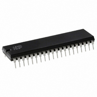
IC 80C51 MCU 256 RAM 40DIP
Manufacturer
NXP Semiconductors
Series
87Cr
Datasheet
1.P87C52X2BN112.pdf
(62 pages)
Specifications of P87C52X2FN,112
Core Processor
8051
Core Size
8-Bit
Speed
33MHz
Connectivity
EBI/EMI, UART/USART
Peripherals
POR
Number Of I /o
32
Program Memory Size
8KB (8K x 8)
Program Memory Type
OTP
Ram Size
256 x 8
Voltage - Supply (vcc/vdd)
2.7 V ~ 5.5 V
Oscillator Type
Internal
Operating Temperature
-40°C ~ 85°C
Package / Case
40-DIP (0.600", 15.24mm)
Processor Series
P87C5x
Core
80C51
Data Bus Width
8 bit
Data Ram Size
256 B
Interface Type
UART
Maximum Clock Frequency
33 MHz
Number Of Programmable I/os
32
Number Of Timers
3
Operating Supply Voltage
2.7 V to 5.5 V
Maximum Operating Temperature
+ 85 C
Mounting Style
SMD/SMT
3rd Party Development Tools
PK51, CA51, A51, ULINK2
Minimum Operating Temperature
- 40 C
Package
40PDIP
Device Core
80C51
Family Name
87C
Maximum Speed
33 MHz
Lead Free Status / RoHS Status
Lead free / RoHS Compliant
Eeprom Size
-
Data Converters
-
Lead Free Status / Rohs Status
Details
Other names
935269602112
P87C52X2FN
P87C52X2FN
P87C52X2FN
P87C52X2FN


1. Absent in the TSSOP38 package.
Philips Semiconductors
NOTES:
To avoid “latch-up” effect at power-on, the voltage on any pin at any time must not be higher than V
2003 Jan 24
PSEN
EA/V
XTAL1
XTAL2
MNEMONIC
80C51 8-bit microcontroller family
4K/8K/16K/32K ROM/OTP, low voltage (2.7 to 5.5 V),
low power, high speed (30/33 MHz)
PP
DIP
29
31
19
18
PLCC
PIN NUMBER
32
35
21
20
LQFP
26
29
15
14
TSSOP
18
20
8
7
TYPE
O
O
I
I
NAME AND FUNCTION
Program Store Enable: The read strobe to external program memory. When the
device is executing code from the external program memory, PSEN is activated
twice each machine cycle, except that two PSEN activations are skipped during
each access to external data memory. PSEN is not activated during fetches from
internal program memory.
External Access Enable/Programming Supply Voltage: EA must be externally held low to enable
the device to fetch code from external program memory locations 0000H to
0FFFH/1FFFH/3FFFH/7FFFH. If EA is held high, the device executes from internal program memory
unless the program counter contains an address greater than the on-chip ROM/OTP. This pin also
receives the 12.75 V programming supply voltage (V
1 is programmed, EA will be internally latched on Reset.
Crystal 1: Input to the inverting oscillator amplifier and input to the internal clock
generator circuits.
Crystal 2: Output from the inverting oscillator amplifier.
11
CC
P80C3xX2; P80C5xX2;
+ 0.5 V or V
PP
) during EPROM programming. If security bit
SS
– 0.5 V, respectively.
P87C5xX2
Product data
Related parts for P87C52X2FN,112
Image
Part Number
Description
Manufacturer
Datasheet
Request
R

Part Number:
Description:
80C51 8-bit microcontrollers 16K/32K, 512 OTP, I2C, watchdog timer
Manufacturer:
PHILIPS [NXP Semiconductors]
Datasheet:

Part Number:
Description:
NXP Semiconductors designed the LPC2420/2460 microcontroller around a 16-bit/32-bitARM7TDMI-S CPU core with real-time debug interfaces that include both JTAG andembedded trace
Manufacturer:
NXP Semiconductors
Datasheet:

Part Number:
Description:
NXP Semiconductors designed the LPC2458 microcontroller around a 16-bit/32-bitARM7TDMI-S CPU core with real-time debug interfaces that include both JTAG andembedded trace
Manufacturer:
NXP Semiconductors
Datasheet:
Part Number:
Description:
NXP Semiconductors designed the LPC2468 microcontroller around a 16-bit/32-bitARM7TDMI-S CPU core with real-time debug interfaces that include both JTAG andembedded trace
Manufacturer:
NXP Semiconductors
Datasheet:
Part Number:
Description:
NXP Semiconductors designed the LPC2470 microcontroller, powered by theARM7TDMI-S core, to be a highly integrated microcontroller for a wide range ofapplications that require advanced communications and high quality graphic displays
Manufacturer:
NXP Semiconductors
Datasheet:
Part Number:
Description:
NXP Semiconductors designed the LPC2478 microcontroller, powered by theARM7TDMI-S core, to be a highly integrated microcontroller for a wide range ofapplications that require advanced communications and high quality graphic displays
Manufacturer:
NXP Semiconductors
Datasheet:
Part Number:
Description:
The Philips Semiconductors XA (eXtended Architecture) family of 16-bit single-chip microcontrollers is powerful enough to easily handle the requirements of high performance embedded applications, yet inexpensive enough to compete in the market for hi
Manufacturer:
NXP Semiconductors
Datasheet:
Part Number:
Description:
The XA-S3 device is a member of Philips Semiconductors? XA(eXtended Architecture) family of high performance 16-bitsingle-chip microcontrollers
Manufacturer:
NXP Semiconductors
Datasheet:

Part Number:
Description:
The NXP BlueStreak LH75401/LH75411 family consists of two low-cost 16/32-bit System-on-Chip (SoC) devices
Manufacturer:
NXP Semiconductors
Datasheet:
Part Number:
Description:
The NXP LPC3130/3131 combine an 180 MHz ARM926EJ-S CPU core, high-speed USB2
Manufacturer:
NXP Semiconductors
Datasheet:
Part Number:
Description:
The NXP LPC3141 combine a 270 MHz ARM926EJ-S CPU core, High-speed USB 2
Manufacturer:
NXP Semiconductors
Part Number:
Description:
The NXP LPC3143 combine a 270 MHz ARM926EJ-S CPU core, High-speed USB 2
Manufacturer:
NXP Semiconductors

Part Number:
Description:
The NXP LPC3152 combines an 180 MHz ARM926EJ-S CPU core, High-speed USB 2
Manufacturer:
NXP Semiconductors
Part Number:
Description:
The NXP LPC3154 combines an 180 MHz ARM926EJ-S CPU core, High-speed USB 2
Manufacturer:
NXP Semiconductors