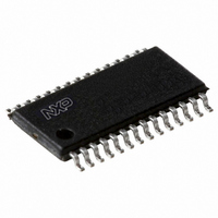
P89LPC935FDH,529 NXP Semiconductors, P89LPC935FDH,529 Datasheet - Page 55

P89LPC935FDH,529
Manufacturer Part Number
P89LPC935FDH,529
Description
IC 80C51 MCU FLASH 8K 28-TSSOP
Manufacturer
NXP Semiconductors
Series
LPC900r
Datasheet
1.P89LPC936FDH518.pdf
(77 pages)
Specifications of P89LPC935FDH,529
Program Memory Type
FLASH
Program Memory Size
8KB (8K x 8)
Package / Case
28-TSSOP
Core Processor
8051
Core Size
8-Bit
Speed
12MHz
Connectivity
I²C, SPI, UART/USART
Peripherals
Brown-out Detect/Reset, LED, POR, PWM, WDT
Number Of I /o
26
Eeprom Size
512 x 8
Ram Size
768 x 8
Voltage - Supply (vcc/vdd)
2.4 V ~ 3.6 V
Data Converters
A/D 8x8b; D/A 2x8b
Oscillator Type
Internal
Operating Temperature
-40°C ~ 85°C
Processor Series
P89LPC9x
Core
80C51
Data Bus Width
8 bit
Data Ram Size
768 B
Interface Type
I2C/SPI/UART
Maximum Clock Frequency
18 MHz
Number Of Programmable I/os
26
Number Of Timers
2
Operating Supply Voltage
2.4 V to 3.6 V
Maximum Operating Temperature
+ 85 C
Mounting Style
SMD/SMT
3rd Party Development Tools
PK51, CA51, A51, ULINK2
Minimum Operating Temperature
- 40 C
On-chip Adc
8-ch x 8-bit
Package
28TSSOP
Device Core
80C51
Family Name
89LP
Maximum Speed
18 MHz
Lead Free Status / RoHS Status
Lead free / RoHS Compliant
For Use With
OM11004 - KIT IAR KICKSTART LPC935622-1014 - BOARD FOR LPC9XX TSSOP622-1008 - BOARD FOR LPC9103 10-HVSON622-1006 - SOCKET ADAPTER BOARDMCB900K - BOARD PROTOTYPE NXP 89LPC9EPM900K - EMULATOR/PROGRAMMER NXP P89LPC9568-4000 - DEMO BOARD SPI/I2C TO DUAL UART568-3510 - DEMO BOARD SPI/I2C TO UART622-1002 - USB IN-CIRCUIT PROG LPC9XX568-1759 - EMULATOR DEBUGGER/PROGRMMR LPC9X568-1758 - BOARD EVAL FOR LPC93X MCU FAMILY
Lead Free Status / Rohs Status
Lead free / RoHS Compliant
Other names
568-1288-5
935274646529
P89LPC935FDH-S
935274646529
P89LPC935FDH-S
NXP Semiconductors
P89LPC933_934_935_936
Product data sheet
9.5.3 Edge triggered
9.5.4 Dual start immediately (P89LPC935/936)
9.6 Boundary limits interrupt
9.7 DAC output to a port pin with high output impedance
9.8 Clock divider
9.9 Power-down and Idle mode
An A/D conversion is started by rising or falling edge of P1.4. Once a conversion has
started, additional edge triggers are ignored until the conversion has completed. The edge
triggered start mode is available in all A/D operating modes.
Programming this mode starts a synchronized conversion of both A/D converters. This
start mode is available in all A/D operating modes. Both A/D converters must be in the
same operating mode. In the continuous conversion modes, both A/D converters must
select an identical number of channels. Any trigger of either A/D will start a simultaneous
conversion of both A/Ds.
Each of the A/D converters has both a high and low boundary limit register. After the four
MSBs have been converted, these four bits are compared with the four MSBs of the
boundary high and low registers. If the four MSBs of the conversion are outside the limit
an interrupt will be generated, if enabled. If the conversion result is within the limits, the
boundary limits will again be compared after all 8 bits have been converted. An interrupt
will be generated, if enabled, if the result is outside the boundary limits. The boundary limit
may be disabled by clearing the boundary limit interrupt enable.
Each A/D converter’s DAC block can be output to a port pin. In this mode, the ADxDAT3
register is used to hold the value fed to the DAC. After a value has been written to the
DAC (written to ADxDAT3), the DAC output will appear on the channel 3 pin.
The A/D converter requires that its internal clock source be in the range of 500 kHz to
3.3 MHz to maintain accuracy. A programmable clock divider that divides the clock
from 1 to 8 is provided for this purpose.
In Idle mode the A/C converter, if enabled, will continue to function and can cause the
device to exit Idle mode when the conversion is completed if the A/D interrupt is enabled.
In Power-down mode or Total Power-down mode, the A/D does not function. If the A/D is
enabled, it will consume power. Power can be reduced by disabling the A/D.
All information provided in this document is subject to legal disclaimers.
Rev. 8 — 12 January 2011
8-bit microcontroller with accelerated two-clock 80C51 core
P89LPC933/934/935/936
© NXP B.V. 2011. All rights reserved.
55 of 77


