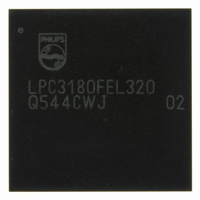
LPC3180FEL320 NXP Semiconductors, LPC3180FEL320 Datasheet - Page 25

LPC3180FEL320
Manufacturer Part Number
LPC3180FEL320
Description
IC ARM9 MCU 208MHZ 320-LFBGA
Manufacturer
NXP Semiconductors
Series
LPC3000r
Datasheet
1.LPC3180FEL320.pdf
(36 pages)
Specifications of LPC3180FEL320
Core Size
16/32-Bit
Oscillator Type
External
Core Processor
ARM9
Speed
208MHz
Connectivity
EBI/EMI, I²C, MMC, SPI, UART/USART, USB OTG
Peripherals
DMA, PWM, WDT
Number Of I /o
55
Program Memory Type
ROMless
Ram Size
64K x 8
Voltage - Supply (vcc/vdd)
1.1 V ~ 3.3 V
Data Converters
A/D 3x10b
Operating Temperature
-40°C ~ 85°C
Package / Case
320-LFBGA
No. Of I/o's
55
Ram Memory Size
64KB
Cpu Speed
208MHz
No. Of Timers
1
No. Of Pwm Channels
2
Digital Ic Case Style
LFBGA
Supply Voltage Range
1.7V
Controller Family/series
LPC31xx
Rohs Compliant
Yes
Lead Free Status / RoHS Status
Lead free / RoHS Compliant
For Use With
622-1018 - EVAL KIT FOR LP3180568-4063 - KIT DEV LPC3180568-4062 - DEBUGGER J-LINK JTAG568-4061 - DEBUGGER U-LINK2 JTAG FOR NXP
Eeprom Size
-
Program Memory Size
-
Lead Free Status / RoHS Status
Lead free / RoHS Compliant, Lead free / RoHS Compliant
Other names
568-3242
Available stocks
Company
Part Number
Manufacturer
Quantity
Price
Company:
Part Number:
LPC3180FEL320
Manufacturer:
NXP Semiconductors
Quantity:
10 000
Company:
Part Number:
LPC3180FEL320,551
Manufacturer:
NXP Semiconductors
Quantity:
10 000
Company:
Part Number:
LPC3180FEL320/01,5
Manufacturer:
NXP Semiconductors
Quantity:
10 000
Company:
Part Number:
LPC3180FEL320551
Manufacturer:
NXP Semiconductors
Quantity:
135
NXP Semiconductors
LPC3180_2
Preliminary data sheet
6.24.1 Crystal oscillator
6.24.2 PLLs
6.23 Reset
6.24 Clocking and power control
Reset is accomplished by an active low signal on the RESET_N input pin. A reset pulse
with a minimum width of 10 main oscillator clocks after the oscillator is stable is required to
guarantee a valid chip reset. At power-up, 10 milliseconds should be allowed for the
oscillator to start up and stabilize after V
with a minimum duration of 10 clock pulses will also be applied if the watchdog timer
generates an internal device reset.
Clocking in the LPC3180 is designed to be versatile, so that system and peripheral
requirements may be met, while allowing optimization of power consumption. Clocks to
most functions may be turned off if not needed, some peripherals do this automatically.
The LPC3180 includes three operational modes that give control over processing speed
and power consumption. In addition, clock rates to different functional blocks may be
controlled by changing clock sources, reconfiguring PLL values, or altering clock divider
configurations. This allows a trade-off of power versus processing speed based on
application requirements.
The main oscillator is the basis for the clocks most chip functions use by default.
Optionally, many functions can be clocked instead by the output of a PLL (with a fixed
397x rate multiplication) which runs from the RTC oscillator. In this mode, the main
oscillator may be turned off unless the USB interface is enabled. If a SYSCLK frequency
other than 13 MHz is required in the application, or if the USB block is not used, the main
oscillator may be used with a frequency of between 1 MHz and 20 MHz.
The LPC3180 includes three PLLs: one allows boosting the RTC frequency to
13.008896 MHz for use as the primary system clock; one provides the 48 MHz clock
required by the USB block; and one provides the basis for the CPU clock, the AHB bus
clock, and the main peripheral clock.
The first PLL multiplies the 32768 Hz RTC clock by 397 to obtain a 13.008896 MHz clock.
The 397x PLL is designed for low power operation and low jitter. This PLL requires an
external RC loop filter for proper operation.
The other two PLLs accept an input clock from either the main oscillator or the output of
the 397x PLL. The input frequency is multiplied up to a higher frequency, then divided
down to provide the output clock.
The PLL input may initially be divided down by a pre-divider value ‘N’, which may have the
values 1, 2, 3, or 4. This pre-divider can allow a greater number of possibilities for the
output frequency.
Following the PLL input divider is the PLL multiplier. This can multiply the pre-divider
output by a value ‘M’, in the range of 1 through 256. The resulting frequency must be in
the range of 156 MHz to 320 MHz. The multiplier works by dividing the output of a Current
Controlled Oscillator (CCO) by the value of M, then using a phase detector to compare the
divided CCO output to the pre-divider output. The error value is used to adjust the CCO
frequency.
Rev. 02 — 15 February 2007
16/32-bit ARM microcontroller with external memory interface
DD
reaches operational voltage. An internal reset
LPC3180
© NXP B.V. 2007. All rights reserved.
25 of 36


