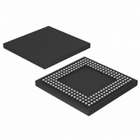
LPC2888FET180/D1,5 NXP Semiconductors, LPC2888FET180/D1,5 Datasheet - Page 23

LPC2888FET180/D1,5
Manufacturer Part Number
LPC2888FET180/D1,5
Description
IC ARM7 MCU 16K 180-TFBGA
Manufacturer
NXP Semiconductors
Series
LPC2800r
Datasheet
1.LPC2888FET180015.pdf
(43 pages)
Specifications of LPC2888FET180/D1,5
Core Processor
ARM7
Core Size
16/32-Bit
Speed
60MHz
Connectivity
EBI/EMI, I²C, IrDA, MMC, UART/USART, USB
Peripherals
DMA, I²S, LCD, WDT
Number Of I /o
85
Program Memory Size
1MB (1M x 8)
Program Memory Type
FLASH
Ram Size
64K x 8
Voltage - Supply (vcc/vdd)
1.7 V ~ 3.6 V
Data Converters
A/D 5x10b
Oscillator Type
External
Operating Temperature
-40°C ~ 85°C
Package / Case
180-TFBGA
Processor Series
LPC28
Core
ARM7TDMI-S
Data Bus Width
32 bit
Data Ram Size
64 KB
Interface Type
I2C, I2S, UART, USB
Maximum Clock Frequency
60 MHz
Number Of Programmable I/os
81
Number Of Timers
2
Operating Supply Voltage
1.8 V, 3.3 V
Maximum Operating Temperature
+ 85 C
Mounting Style
SMD/SMT
3rd Party Development Tools
MDK-ARM, RL-ARM, ULINK2
Development Tools By Supplier
OM10092
Minimum Operating Temperature
- 40 C
On-chip Adc
10 bit, 5 Channel
For Use With
OM10092 - EVAL BOARD FOR LPC288X
Lead Free Status / RoHS Status
Lead free / RoHS Compliant
Eeprom Size
-
Lead Free Status / Rohs Status
Details
Other names
935285219551
LPC2888FET180/D1-S
LPC2888FET180/D1-S
LPC2888FET180/D1-S
LPC2888FET180/D1-S
NXP Semiconductors
LPC2880_LPC2888_3
Preliminary data sheet
6.20.1 Features
6.21.1 Features
6.21.2 Reset
6.20 LCD interface
6.21 Clocking and power control
The LCD interface contains logic to interface to a 6800 or 8080 bus compatible LCD
controller. The LCD interface is compatible with the 6800 bus standard and the 8080 bus
standard, with one address pin (RS) for selecting the data or instruction register.
The LCD interface makes use of a configurable clock (programmed in the CGU) to adjust
the speed of the 6800/8080 bus to the speed of the connected peripheral.
Clocking in the LPC2880/2888 is controlled by a versatile CGU, so that system and
peripheral requirements may be met while allowing optimization of power consumption.
Clocks to most functions may be turned off if not needed, and may be enabled and
disabled by selected events through the Event Router.
Clock sources include a high frequency (1 MHz to 20 MHz) crystal oscillator and a 32 kHz
RTC oscillator. Higher frequency clocks may be generated through the use of two
programmable PLLs.
Reset of individual functional blocks is also controlled by the CGU. Full chip reset can be
initiated by the external reset pin or by the watchdog timer.
The LPC2880/2888 has two sources of reset: the RESET pin and the watchdog reset. The
RESET pin includes an on-chip pull-up. RESET must remain low at power-up for 1 ms
after power supply voltages are stable. This includes on-chip DC-to-DC converter
voltages.
When either reset is removed, the processor begins executing at address 0, which is the
reset vector. At that point, all of the processor and peripheral registers have been
initialized to predetermined values.
•
•
•
•
•
•
•
•
•
8-bit or 4-bit parallel interface mode: 6800-series, 8080-series.
Selectable bus frequency supports high and low speed LCD controllers.
Supports polling the busy flag from the LCD controller to avoid CPU polling.
Contains a 16 B FIFO for sending control and data information to the LCD controller.
Contains a serial interface which uses the same FIFO for serial transmissions.
Supports FIFO level flow control to the General Purpose DMA controller.
Power and performance control provided by versatile clock generation to individual
functional blocks.
Multiple clock sources including external crystal and programmable PLLs.
Individual control of software reset to many functional blocks.
16/32-bit ARM microcontrollers with external memory interface
Rev. 03 — 17 April 2008
LPC2880; LPC2888
© NXP B.V. 2008. All rights reserved.
23 of 43


