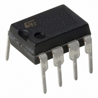
ST7FLITEU05B6 STMicroelectronics, ST7FLITEU05B6 Datasheet - Page 101

ST7FLITEU05B6
Manufacturer Part Number
ST7FLITEU05B6
Description
MCU 8BIT SGL VOLT FLASH 8-DIP
Manufacturer
STMicroelectronics
Series
ST7r
Datasheet
1.ST7FLITEU05M6.pdf
(139 pages)
Specifications of ST7FLITEU05B6
Core Processor
ST7
Core Size
8-Bit
Speed
8MHz
Peripherals
LVD, POR, PWM, WDT
Number Of I /o
5
Program Memory Size
2KB (2K x 8)
Program Memory Type
FLASH
Ram Size
128 x 8
Voltage - Supply (vcc/vdd)
2.4 V ~ 5.5 V
Data Converters
A/D 5x10b
Oscillator Type
Internal
Operating Temperature
-40°C ~ 85°C
Package / Case
8-DIP (0.300", 7.62mm)
Processor Series
ST7FLITEUx
Core
ST7
Data Bus Width
8 bit
Data Ram Size
128 B
Interface Type
ICC
Maximum Clock Frequency
4 MHz
Number Of Programmable I/os
5
Number Of Timers
2
Maximum Operating Temperature
+ 85 C
Mounting Style
Through Hole
Development Tools By Supplier
ST7FUS-PRIMER, ST7FLITE-SK/RAIS, ST7FLITU0-D/RAIS, STX-RLINK
Minimum Operating Temperature
- 40 C
On-chip Adc
10 bit, 5 Channel
For Use With
497-5858 - EVAL BOARD PLAYBACK ST7FLITE
Lead Free Status / RoHS Status
Lead free / RoHS Compliant
Eeprom Size
-
Connectivity
-
Lead Free Status / Rohs Status
Details
ST7LITEU05 ST7LITEU09
13.4
13.4.1
Table 54.
1. CPU running with memory access, all I/O pins in input mode with a static value at V
2. Data based on characterization, not tested in production.
3.
4. Slow mode selected with fCPU based on fOSC divided by 32. All I/O pins in input mode with a static value at V
5.
6. All I/O pins in input mode with a static value at V
7. This consumption refers to the Halt period only and not the associated run period which is software dependent.
8. All I/O pins in output mode with a static value at VSS (no load), LVD disabled. Data based on characterization results,
Symbol
I
reset state; clock input (CLKIN) driven by external square wave, LVD disabled.
driven by external square wave, LVD disabled.
(no load), all peripherals in reset state; clock input (CLKIN) driven by external square wave, LVD disabled.
V
tested in production at V
DD
All I/O pins in input mode with a static value at VDD or VSS (no load), all peripherals in reset state; clock input (CLKIN)
Slow-Wait mode selected with fCPU based on fOSC divided by 32. All I/O pins in input mode with a static value at V
SS
(no load), all peripherals in reset state; clock input (CLKIN) driven by external square wave, LVD disabled.
Supply current in RUN mode
Supply current in Wait mode
Supply current in Slow mode
Supply current in Slow-Wait mode
Supply current in AWUFH mode
Supply current in ACTIVE Halt mode
Supply current in Halt mode
Supply current in RUN mode
Supply current in Wait mode
Supply current in Slow mode
Supply current in Slow-wait mode
Supply current in AWUFH mode
Supply current in ACTIVE Halt mode
Supply current in Halt mode
Supply current characteristics
The following current consumption specified for the ST7 functional operating modes over
temperature range does not take into account the clock source current consumption. To get
the total device consumption, the two current values must be added (except for Halt mode
for which the clock is stopped). Refer to
characteristics on page
Supply current
T
Supply current characteristics
A
= -40 to +125°C unless otherwise specified
Parameter
DD
max and f
CPU
(3)
(8)
(8)
(3)
(1)
(4)
(1)
(4)
102.
max.
(6)(7)
(6)(7)
(5)
(5)
DD
or V
SS
(no load). Data tested in production at V
f
f
f
f
f
f
T
T
f
f
f
f
T
T
CPU
CPU
CPU
CPU
CPU
CPU
CPU
CPU
CPU
CPU
A
A
A
A
Section 13.4.2: Internal RC oscillator supply
= 85
= 125
= 85
= 125
/32 = 250 kHz
/32 = 250 kHz
/32 = 250 kHz
/32 = 250 kHz
= 4 MHz
= 8 MHz
= 4 MHz
= 8 MHz
= 4 MHz
= 4 MHz
Conditions
°C
°C
°C
°C
DD
or V
SS
Electrical characteristics
(no load), all peripherals in
DD
0.85
1.30
0.36
0.25
0.25
Typ
600
450
100
300
250
2.5
5.0
1.2
0.5
0.5
45
20
90
max. and f
100
2.0
400
350
150
2.5
4.5
0.5
4.5
2.0
50
Max
950
750
250
7.5
3.5
3.0
5.0
DD
CPU
(2)
(2)
(2)
(2)
(2)
(2)
(2)
(2)
(2)
(2)
(2)
or V
DD
max.
101/139
SS
Unit
or
mA
mA
A
A


