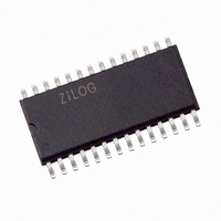
Z8F0412SJ020SG Zilog, Z8F0412SJ020SG Datasheet - Page 144

Z8F0412SJ020SG
Manufacturer Part Number
Z8F0412SJ020SG
Description
IC ENCORE MCU FLASH 4K 28SOIC
Manufacturer
Zilog
Series
Encore!® XP®r
Datasheet
1.Z8F08200100KIT.pdf
(264 pages)
Specifications of Z8F0412SJ020SG
Core Processor
Z8
Core Size
8-Bit
Speed
20MHz
Connectivity
I²C, IrDA, SPI, UART/USART
Peripherals
Brown-out Detect/Reset, POR, PWM, WDT
Number Of I /o
19
Program Memory Size
4KB (4K x 8)
Program Memory Type
FLASH
Ram Size
1K x 8
Voltage - Supply (vcc/vdd)
2.7 V ~ 3.6 V
Oscillator Type
Internal
Operating Temperature
0°C ~ 70°C
Package / Case
28-SOIC (7.5mm Width)
Processor Series
Z8F041xx
Core
eZ8
Data Bus Width
8 bit
Data Ram Size
1 KB
Interface Type
I2C, SPI, UART
Maximum Clock Frequency
20 MHz
Number Of Programmable I/os
19
Number Of Timers
2
Operating Supply Voltage
2.7 V to 3.6 V
Maximum Operating Temperature
+ 70 C
Mounting Style
SMD/SMT
Minimum Operating Temperature
0 C
Lead Free Status / RoHS Status
Lead free / RoHS Compliant
Eeprom Size
-
Data Converters
-
Lead Free Status / Rohs Status
Details
Other names
269-4107
Z8F0412SJ020SG
Z8F0412SJ020SG
Available stocks
Company
Part Number
Manufacturer
Quantity
Price
Part Number:
Z8F0412SJ020SG
Manufacturer:
ZILOG
Quantity:
20 000
- Current page: 144 of 264
- Download datasheet (6Mb)
PS022517-0508
Address Only Transaction with a 7-bit Address
When reading data from the slave, the I
the receive interrupt is serviced and the
the I
data byte.
In the situation where software determines if a slave with a 7-bit address is responding
without sending or receiving data, a transaction can be done which only consists of an
address phase.
if a slave with a 7-bit address will acknowledge. As an example, this transaction can be
used after a “write” has been done to a EEPROM to determine when the EEPROM com-
pletes its internal write operation and is once again responding to I
slave does not Acknowledge, the transaction is repeated until the slave does Acknowl-
edge.
Follow the steps below for an address only transaction to a 7-bit addressed slave:
1. Software asserts the IEN bit in the I
2. Software asserts the TXI bit of the I
3. The I
4. Software responds to the TDRE bit by writing a 7-bit Slave address plus write bit (=0)
5. Software sets the START and STOP bits of the I
6. The I
7. The I
8. Software polls the STOP bit of the I
9.
to the I
write operation.
TXI bit.
Register.
STOP bit when the address only transaction is completed.
the ACK bit is equal to 1. If the slave does not acknowledge, the ACK bit is equal to 0.
The NCKI interrupt does not occur in the not acknowledge case because the STOP bit
was set.
2
Software checks the ACK bit of the I
C Data Register. Once the I
2
2
2
Figure 26. 7-Bit Address Only Transaction Format
C interrupt asserts, because the I
C Controller sends the START condition to the I
C Controller loads the I
2
C Data Register. As an alternative this could be a read operation instead of a
Figure 26
S
Slave Address
on page 131 displays this “address only” transaction to determine
2
C Data Register has been read, the I
2
C Shift register with the contents of the I
W = 0 A/A
RDRF
2
2
2
2
C pauses after the data Acknowledge cycle until
C Control Register. Hardware deasserts the
C Control Register.
C Control Register to enable Transmit interrupts.
2
2
C Status Register. If the slave acknowledged,
C Data Register is empty (TDRE = 1)
bit of the status register is cleared by reading
2
C Control Register and clears the
P
Z8 Encore! XP
2
C Slave.
Product Specification
2
C transactions. If the
2
C reads the next
®
F0822 Series
2
C Data
I2C Controller
131
Related parts for Z8F0412SJ020SG
Image
Part Number
Description
Manufacturer
Datasheet
Request
R

Part Number:
Description:
Communication Controllers, ZILOG INTELLIGENT PERIPHERAL CONTROLLER (ZIP)
Manufacturer:
Zilog, Inc.
Datasheet:

Part Number:
Description:
KIT DEV FOR Z8 ENCORE 16K TO 64K
Manufacturer:
Zilog
Datasheet:

Part Number:
Description:
KIT DEV Z8 ENCORE XP 28-PIN
Manufacturer:
Zilog
Datasheet:

Part Number:
Description:
DEV KIT FOR Z8 ENCORE 8K/4K
Manufacturer:
Zilog
Datasheet:

Part Number:
Description:
KIT DEV Z8 ENCORE XP 28-PIN
Manufacturer:
Zilog
Datasheet:

Part Number:
Description:
DEV KIT FOR Z8 ENCORE 4K TO 8K
Manufacturer:
Zilog
Datasheet:

Part Number:
Description:
CMOS Z8 microcontroller. ROM 16 Kbytes, RAM 256 bytes, speed 16 MHz, 32 lines I/O, 3.0V to 5.5V
Manufacturer:
Zilog, Inc.
Datasheet:

Part Number:
Description:
Low-cost microcontroller. 512 bytes ROM, 61 bytes RAM, 8 MHz
Manufacturer:
Zilog, Inc.
Datasheet:

Part Number:
Description:
Z8 4K OTP Microcontroller
Manufacturer:
Zilog, Inc.
Datasheet:

Part Number:
Description:
CMOS SUPER8 ROMLESS MCU
Manufacturer:
Zilog, Inc.
Datasheet:

Part Number:
Description:
SL1866 CMOSZ8 OTP Microcontroller
Manufacturer:
Zilog, Inc.
Datasheet:

Part Number:
Description:
SL1866 CMOSZ8 OTP Microcontroller
Manufacturer:
Zilog, Inc.
Datasheet:

Part Number:
Description:
OTP (KB) = 1, RAM = 125, Speed = 12, I/O = 14, 8-bit Timers = 2, Comm Interfaces Other Features = Por, LV Protect, Voltage = 4.5-5.5V
Manufacturer:
Zilog, Inc.
Datasheet:

Part Number:
Description:
Manufacturer:
Zilog, Inc.
Datasheet:


