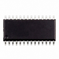
ST62T25CM6 STMicroelectronics, ST62T25CM6 Datasheet - Page 81

ST62T25CM6
Manufacturer Part Number
ST62T25CM6
Description
IC MCU 8BIT OTP 4K 28 SOIC
Manufacturer
STMicroelectronics
Series
ST6r
Datasheet
1.ST62T25CB6.pdf
(100 pages)
Specifications of ST62T25CM6
Core Processor
ST6
Core Size
8-Bit
Speed
8MHz
Peripherals
LVD, POR, WDT
Number Of I /o
20
Program Memory Size
4KB (4K x 8)
Program Memory Type
OTP
Ram Size
64 x 8
Voltage - Supply (vcc/vdd)
3 V ~ 6 V
Data Converters
A/D 16x8b
Oscillator Type
Internal
Operating Temperature
-40°C ~ 85°C
Package / Case
28-SOIC (7.5mm Width)
Processor Series
ST62T2x
Core
ST6
Data Bus Width
8 bit
Data Ram Size
64 B
Maximum Clock Frequency
8 MHz
Number Of Programmable I/os
20
Number Of Timers
2
Operating Supply Voltage
3 V to 6 V
Maximum Operating Temperature
+ 85 C
Mounting Style
SMD/SMT
Development Tools By Supplier
ST62GP-EMU2, ST62E2XC-EPB/110, ST62E6XC-EPB/US, ST622XC-KIT/110, STREALIZER-II
Minimum Operating Temperature
- 40 C
On-chip Adc
8 bit
Lead Free Status / RoHS Status
Contains lead / RoHS non-compliant
Eeprom Size
-
Connectivity
-
Lead Free Status / Rohs Status
Details
Other names
497-2101-5
Available stocks
Company
Part Number
Manufacturer
Quantity
Price
Part Number:
ST62T25CM6
Manufacturer:
ST
Quantity:
20 000
EMC CHARACTERISTICS (Cont’d)
11.7.3 ESD Pin Protection Strategy
To protect an integrated circuit against Electro-
Static Discharge the stress must be controlled to
prevent degradation or destruction of the circuit el-
ements. The stress generally affects the circuit el-
ements which are connected to the pads but can
also affect the internal devices when the supply
pads receive the stress. The elements to be pro-
tected must not receive excessive current, voltage
or heating within their structure.
An ESD network combines the different input and
output ESD protections. This network works, by al-
lowing safe discharge paths for the pins subjected
to ESD stress. Two critical ESD stress cases are
presented in
pins.
Figure 59. Positive Stress on a Standard Pad vs. V
Figure 60. Negative Stress on a Standard Pad vs. V
Main path
Path to avoid
Main path
Figure 59
V
V
V
V
DD
DD
SS
SS
and
Figure 60
(3a)
(3b)
(3a)
(3b)
for standard
OUT
OUT
SS
Standard Pin Protection
To protect the output structure the following ele-
ments are added:
– A diode to V
– A protection device between V
To protect the input structure the following ele-
ments are added:
– A resistor in series with the pad (1)
– A diode to V
– A protection device between V
DD
(4)
(4)
ST6215CM-Auto ST6225CM-Auto
IN
IN
DD
DD
(3a) and a diode from V
(2a) and a diode from V
(2a)
(2b)
(2a)
(2b)
(1)
(1)
DD
DD
and V
and V
SS
SS
SS
SS
81/100
V
V
V
V
(3b)
(2b)
(4)
(4)
DD
SS
DD
SS
1


