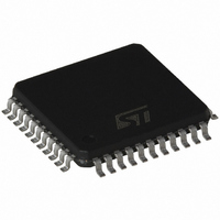
ST72F361J7T3 STMicroelectronics, ST72F361J7T3 Datasheet - Page 101

ST72F361J7T3
Manufacturer Part Number
ST72F361J7T3
Description
IC MCU 8BIT 48K FLASH 44-LQFP
Manufacturer
STMicroelectronics
Series
ST7r
Datasheet
1.ST72F361K6T6.pdf
(225 pages)
Specifications of ST72F361J7T3
Core Processor
ST7
Core Size
8-Bit
Speed
8MHz
Connectivity
LINSCI, SPI
Peripherals
LVD, POR, PWM, WDT
Number Of I /o
32
Program Memory Size
48KB (48K x 8)
Program Memory Type
FLASH
Ram Size
2K x 8
Voltage - Supply (vcc/vdd)
3.8 V ~ 5.5 V
Data Converters
A/D 16x10b
Oscillator Type
External
Operating Temperature
-40°C ~ 125°C
Package / Case
44-LQFP
Processor Series
ST72F3x
Core
ST7
Data Bus Width
8 bit
Data Ram Size
2 KB
Interface Type
LINSCI, SPI
Maximum Clock Frequency
8 MHz
Number Of Programmable I/os
34
Number Of Timers
2
Maximum Operating Temperature
+ 125 C
Mounting Style
SMD/SMT
Development Tools By Supplier
ST72F36X-SK/RAIS, STX-RLINK
Minimum Operating Temperature
- 40 C
On-chip Adc
10 bit, 11 Channel
Lead Free Status / RoHS Status
Lead free / RoHS Compliant
Eeprom Size
-
Lead Free Status / Rohs Status
Details
Available stocks
Company
Part Number
Manufacturer
Quantity
Price
Company:
Part Number:
ST72F361J7T3
Manufacturer:
STMicroelectronics
Quantity:
10 000
- Current page: 101 of 225
- Download datasheet (8Mb)
8-BIT TIMER (Cont’d)
10.5.3.5 Pulse Width Modulation Mode
Pulse Width Modulation (PWM) mode enables the
generation of a signal with a frequency and pulse
length determined by the value of the OC1R and
OC2R registers.
Pulse Width Modulation mode uses the complete
Output Compare 1 function plus the OC2R regis-
ter, and so this functionality can not be used when
PWM mode is activated.
In PWM mode, double buffering is implemented on
the output compare registers. Any new values writ-
ten in the OC1R and OC2R registers are taken
into account only at the end of the PWM period
(OC2) to avoid spikes on the PWM output pin
(OCMP1).
Procedure
To use pulse width modulation mode:
1. Load the OC2R register with the value corre-
2. Load the OC1R register with the value corre-
3. Select the following in the CR1 register:
4. Select the following in the CR2 register:
sponding to the period of the signal using the
formula in the opposite column.
sponding to the period of the pulse if
(OLVL1 = 0 and OLVL2 = 1) using the formula
in the opposite column.
– Using the OLVL1 bit, select the level to be ap-
– Using the OLVL2 bit, select the level to be ap-
– Set OC1E bit: the OCMP1 pin is then dedicat-
– Set the PWM bit.
– Select the timer clock (CC[1:0]) (see
plied to the OCMP1 pin after a successful
comparison with the OC1R register.
plied to the OCMP1 pin after a successful
comparison with the OC2R register.
ed to the output compare 1 function.
Clock Control
Counter
= OC1R
Counter
= OC2R
When
When
Bits).
Pulse Width Modulation cycle
OCMP1 = OLVL2
OCMP1 = OLVL1
Counter is reset
ICF1 bit is set
to FCh
Table 19
If OLVL1 = 1 and OLVL2 = 0 the length of the pos-
itive pulse is the difference between the OC2R and
OC1R registers.
If OLVL1 = OLVL2 a continuous signal will be
seen on the OCMP1 pin.
The OC
ing application can be calculated using the follow-
ing formula:
Where:
t
f
PRESC
The Output Compare 2 event causes the counter
to be initialized to FCh (See
Notes:
1. The OCF1 and OCF2 bits cannot be set by
2. The ICF1 bit is set by hardware when the coun-
3. In PWM mode the ICAP1 pin can not be used
4. When the Pulse Width Modulation (PWM) and
CPU
hardware in PWM mode therefore the Output
Compare interrupt is inhibited.
ter reaches the OC2R value and can produce a
timer interrupt if the ICIE bit is set and the I bit is
cleared.
to perform input capture because it is discon-
nected to the timer. The ICAP2 pin can be used
to perform input capture (ICF2 can be set and
IC2R can be loaded) but the user must take
care that the counter is reset each period and
ICF1 can also generates interrupt if ICIE is set.
One Pulse Mode (OPM) bits are both set, the
PWM mode is the only active one.
= Signal or pulse period (in seconds)
= PLL output x2 clock frequency in hertz
= Timer prescaler factor (2, 4, 8 or 8000
i
R register value required for a specific tim-
OCiR Value =
(or f
depending on CC[1:0] bits, see
19 Clock Control
OSC
/2 if PLL is not enabled)
PRESC
t
Bits)
*
Figure
f
CPU
69)
- 5
ST72361
101/225
Table
Related parts for ST72F361J7T3
Image
Part Number
Description
Manufacturer
Datasheet
Request
R

Part Number:
Description:
STMicroelectronics [RIPPLE-CARRY BINARY COUNTER/DIVIDERS]
Manufacturer:
STMicroelectronics
Datasheet:

Part Number:
Description:
STMicroelectronics [LIQUID-CRYSTAL DISPLAY DRIVERS]
Manufacturer:
STMicroelectronics
Datasheet:

Part Number:
Description:
BOARD EVAL FOR MEMS SENSORS
Manufacturer:
STMicroelectronics
Datasheet:

Part Number:
Description:
NPN TRANSISTOR POWER MODULE
Manufacturer:
STMicroelectronics
Datasheet:

Part Number:
Description:
TURBOSWITCH ULTRA-FAST HIGH VOLTAGE DIODE
Manufacturer:
STMicroelectronics
Datasheet:

Part Number:
Description:
Manufacturer:
STMicroelectronics
Datasheet:

Part Number:
Description:
DIODE / SCR MODULE
Manufacturer:
STMicroelectronics
Datasheet:

Part Number:
Description:
DIODE / SCR MODULE
Manufacturer:
STMicroelectronics
Datasheet:

Part Number:
Description:
Search -----> STE16N100
Manufacturer:
STMicroelectronics
Datasheet:

Part Number:
Description:
Search ---> STE53NA50
Manufacturer:
STMicroelectronics
Datasheet:

Part Number:
Description:
NPN Transistor Power Module
Manufacturer:
STMicroelectronics
Datasheet:

Part Number:
Description:
DIODE / SCR MODULE
Manufacturer:
STMicroelectronics
Datasheet:


