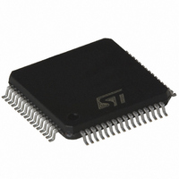
ST72F321AR9TA STMicroelectronics, ST72F321AR9TA Datasheet - Page 12

ST72F321AR9TA
Manufacturer Part Number
ST72F321AR9TA
Description
IC MCU 8BIT 60KB FLASH 64-TQFP
Manufacturer
STMicroelectronics
Series
ST7r
Datasheet
1.ST72F321AR7T6.pdf
(193 pages)
Specifications of ST72F321AR9TA
Core Processor
ST7
Core Size
8-Bit
Speed
8MHz
Connectivity
I²C, SCI, SPI
Peripherals
LVD, POR, PWM, WDT
Number Of I /o
48
Program Memory Size
60KB (60K x 8)
Program Memory Type
FLASH
Ram Size
2K x 8
Voltage - Supply (vcc/vdd)
3.8 V ~ 5.5 V
Data Converters
A/D 16x10b
Oscillator Type
Internal
Operating Temperature
-40°C ~ 85°C
Package / Case
64-TQFP, 64-VQFP
Lead Free Status / RoHS Status
Lead free / RoHS Compliant
Eeprom Size
-
Available stocks
Company
Part Number
Manufacturer
Quantity
Price
Company:
Part Number:
ST72F321AR9TA
Manufacturer:
ST
Quantity:
215
Company:
Part Number:
ST72F321AR9TA
Manufacturer:
STMicroelectronics
Quantity:
10 000
Part Number:
ST72F321AR9TA
Manufacturer:
ST
Quantity:
20 000
Company:
Part Number:
ST72F321AR9TAE
Manufacturer:
STMicroelectronics
Quantity:
10 000
Company:
Part Number:
ST72F321AR9TATR
Manufacturer:
STMicroelectronics
Quantity:
10 000
ST72321Rx ST72321ARx ST72321Jx
Notes:
1. In the interrupt input column, “eiX” defines the associated external interrupt vector. If the weak pull-up
column (wpu) is merged with the interrupt column (int), then the I/O configuration is pull-up interrupt input,
else the configuration is floating interrupt input.
2. In the open drain output column, “T” defines a true open drain I/O (P-Buffer and protection diode to V
are not implemented). See See “I/O PORTS” on page 46. and
12/193
45
46 31 16 PA3 (HS)
47 32
48 33
49 34 17 PA4 (HS)
50 35
51 36 18 PA6 (HS)/SDAI
52 37 19 PA7 (HS)/SCLI
53 38 20 V
54 39 21 RESET
55
56
57 40 22 V
58 41 23 OSC2
59 42 24 OSC1
60 43 25 V
61 44 26 PE0/TDO
62
63
64
Pin n°
1
-
-
-
-
-
27 PE1/RDI
-
-
-
-
-
-
-
-
PA2
V
V
PA5 (HS)
EVD
TLI
PE2 (Flash device)
PE2 (ROM device)
PE3
DD_1
SS_1
PP
SS_2
DD_2
/ ICCSEL
Pin Name
3)
3)
I/O C
I/O C
I/O C
I/O C
I/O C
I/O C
I/O C
I/O
I/O C
I/O C
I/O C
I/O C
S
S
S
S
I
I
I
C
Level
T
T
T
T
T
T
T
T
T
T
T
T
HS
HS
HS
HS
HS
X
X
X
X
X
X
X
X
X
X
X
X
X
X
X
X
Input
ei0
ei0
X
Port
Section 12.8 I/O PORT PIN CHARACTER-
Output
X
X
X
X
X
X
X
X
T
T
X
X
X
X
X
X
X
X
function
Port A2
Port A3
Digital Main Supply Voltage
Digital Ground Voltage
Port A4
Port A5
Port A6
Port A7
Must be tied low. In flash program-
ming mode, this pin acts as the pro-
gramming voltage input V
Section 12.9.2
voltage must not be applied to ROM
devices
Top priority non maskable interrupt.
External voltage detector
Top level interrupt input pin
Digital Ground Voltage
Resonator oscillator inverter output
External clock input or Resonator os-
cillator inverter input
Digital Main Supply Voltage
Port E0
Port E1
Port E2
Caution: In Flash devices this port is
always input with weak pull-up.
Port E2
Caution: In ROM devices, no weak
pull-up present on this port.
In LQFP44 this pin is not connected to
an internal pull-up like other unbond-
ed pins (See note 4). It is recommend-
ed to configure it as output push pull
to avoid added current consumption.
Port E3
reset)
(after
Main
SCI Transmit Data Out
SCI Receive Data In
I
I
2
2
C Data
C Clock
Alternate function
for more details. High
1)
1)
PP
. See
DD


