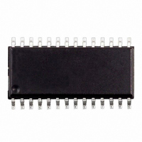
ST62T65CM6 STMicroelectronics, ST62T65CM6 Datasheet - Page 11

ST62T65CM6
Manufacturer Part Number
ST62T65CM6
Description
IC MCU 8BIT OTP/EPROM 28 PSOIC
Manufacturer
STMicroelectronics
Series
ST6r
Datasheet
1.ST62T55CB6.pdf
(84 pages)
Specifications of ST62T65CM6
Core Processor
ST6
Core Size
8-Bit
Speed
8MHz
Connectivity
SPI
Peripherals
LED, LVD, POR, WDT
Number Of I /o
21
Program Memory Size
3.8KB (3.8K x 8)
Program Memory Type
OTP
Eeprom Size
128 x 8
Ram Size
128 x 8
Voltage - Supply (vcc/vdd)
3 V ~ 6 V
Data Converters
A/D 13x8b
Oscillator Type
Internal
Operating Temperature
-40°C ~ 85°C
Package / Case
28-SOIC (7.5mm Width)
Controller Family/series
ST6
No. Of I/o's
21
Eeprom Memory Size
128Byte
Ram Memory Size
128Byte
Cpu Speed
8MHz
No. Of Timers
2
Rohs Compliant
Yes
Processor Series
ST62T6x
Core
ST6
Data Bus Width
8 bit
Data Ram Size
128 B
Interface Type
SCI
Maximum Clock Frequency
8 MHz
Number Of Programmable I/os
21
Number Of Timers
1
Operating Supply Voltage
3 V to 6 V
Maximum Operating Temperature
+ 125 C
Mounting Style
SMD/SMT
Development Tools By Supplier
ST62GP-EMU2, ST62E2XC-EPB/110, ST62E6XC-EPB/US, STREALIZER-II
Minimum Operating Temperature
- 40 C
On-chip Adc
8 bit
Lead Free Status / RoHS Status
Lead free / RoHS Compliant
Other names
497-2103-5
Available stocks
Company
Part Number
Manufacturer
Quantity
Price
Company:
Part Number:
ST62T65CM6
Manufacturer:
ST
Quantity:
700
MEMORY MAP (Cont’d)
Additional Notes on Parallel Mode:
If the user wishes to perform parallel program-
ming, the first step should be to set the E2PAR2
bit. From this time on, the EEPROM will be ad-
dressed in write mode, the ROW address and the
data will be latched and it will be possible to
change them only at the end of the programming
cycle or by resetting E2PAR2 without program-
ming the EEPROM. After the ROW address is
latched, the MCU can only “see” the selected
EEPROM row and any attempt to write or read
other rows will produce errors.
The EEPROM should not be read while E2PAR2
is set.
As soon as the E2PAR2 bit is set, the 8 volatile
ROW latches are cleared. From this moment on,
the user can load data in all or in part of the ROW.
Setting E2PAR1 will modify the EEPROM regis-
ters corresponding to the ROW latches accessed
after E2PAR2. For example, if the software sets
E2PAR2 and accesses the EEPROM by writing to
addresses 18h, 1Ah and 1Bh, and then sets
E2PAR1, these three registers will be modified si-
multaneously; the remaining bytes in the row will
be unaffected.
Note that E2PAR2 is internally reset at the end of
the programming cycle. This implies that the user
must set the E2PAR2 bit between two parallel pro-
gramming cycles. Note that if the user tries to set
E2PAR1 while E2PAR2 is not set, there will be no
programming cycle and the E2PAR1 bit will be un-
affected. Consequently, the E2PAR1 bit cannot be
set if E2ENA is low. The E2PAR1 bit can be set by
the user, only if the E2ENA and E2PAR2 bits are
also set.
Notes: The EEPROM page shall not be changed
through the DRBR register when the E2PAR2 bit
is set.
EEPROM Control Register (EECTL)
Address: EAh — Read/Write
Reset status: 00h
Bit 7 = D7: Unused.
Bit 6 = E2OFF: Stand-by Enable Bit. WRITE ONLY.
If this bit is set the EEPROM is disabled (any access
will be meaningless) and the power consumption of
the EEPROM is reduced to its lowest value.
Bit 5-4 = D5-D4: Reserved. MUST be kept reset.
Bit 3 = E2PAR1: Parallel Start Bit. WRITE ONLY.
Once in Parallel Mode, as soon as the user software
sets the E2PAR1 bit, parallel writing of the 8 adja-
cent registers will start. This bit is internally reset at
the end of the programming procedure. Note that
less than 8 bytes can be written if required, the un-
defined bytes being unaffected by the parallel pro-
gramming cycle; this is explained in greater detail in
the Additional Notes on Parallel Mode overleaf.
Bit 2 = E2PAR2: Parallel Mode En. Bit. WRITE
ONLY. This bit must be set by the user program in
order to perform parallel programming. If E2PAR2
is set and the parallel start bit (E2PAR1) is reset,
up to 8 adjacent bytes can be written simultane-
ously. These 8 adjacent bytes are considered as a
row, whose address lines A7, A6, A5, A4, A3 are
fixed while A2, A1 and A0 are the changing bits, as
illustrated in
set at the end of any parallel programming proce-
dure. It can be reset by the user software before
starting the programming procedure, thus leaving
the EEPROM registers unchanged.
Bit 1 = E2BUSY: EEPROM Busy Bit. READ ON-
LY. This bit is automatically set by the EEPROM
control logic when the EEPROM is in program-
ming mode. The user program should test it before
any EEPROM read or write operation; any attempt
to access the EEPROM while the busy bit is set
will be aborted and the writing procedure in
progress will be completed.
Bit 0 = E2ENA: EEPROM Enable Bit. WRITE ON-
LY. This bit enables programming of the EEPROM
cells. It must be set before any write to the EEP-
ROM register. Any attempt to write to the EEP-
D7
7
E2O
FF
Figure
D5
ST6255C ST6265C ST6265B
D4
4. E2PAR2 is automatically re-
E2PA
R1
E2PA
R2
E2BU
SY
E2E
11/84
NA
0


