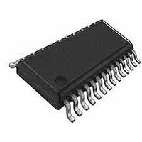
CY8CLED16P01-28PVXIT Cypress Semiconductor Corp, CY8CLED16P01-28PVXIT Datasheet - Page 18

CY8CLED16P01-28PVXIT
Manufacturer Part Number
CY8CLED16P01-28PVXIT
Description
IC PLC PSOC CMOS LED 16CH 28SSOP
Manufacturer
Cypress Semiconductor Corp
Series
PowerPSoC® CY8CLEDr
Datasheet
1.CY8CLED16P01-48LFXI.pdf
(46 pages)
Specifications of CY8CLED16P01-28PVXIT
Package / Case
28-SSOP
Core Processor
M8C
Core Size
8-Bit
Speed
24MHz
Connectivity
I²C, IrDA, SPI, UART/USART
Peripherals
LED, PLC, POR, PWM, WDT
Number Of I /o
24
Program Memory Size
32KB (32K x 8)
Program Memory Type
FLASH
Ram Size
2K x 8
Voltage - Supply (vcc/vdd)
4.75 V ~ 5.25 V
Data Converters
A/D 4x14b; D/A 4x9b
Oscillator Type
Internal
Operating Temperature
-40°C ~ 85°C
Operating Supply Voltage
4.75 V to 5.25 V
Maximum Supply Current
8 mA
Maximum Operating Temperature
+ 85 C
Mounting Style
SMD/SMT
Minimum Operating Temperature
- 40 C
Lead Free Status / RoHS Status
Lead free / RoHS Compliant
Eeprom Size
-
Lead Free Status / Rohs Status
Details
8. Pin Information
The CY8CLED16P01 PLC device is available in a variety of packages which are listed and illustrated in the following tables. Every
port pin (labeled with a “P”) is capable of Digital I/O. However, Vss, Vdd, and XRES are not capable of Digital I/O.
8.1 28-Pin Part Pinout
Table 8-1. 28-Pin Part Pinout (SSOP)
Document Number: 001-49263 Rev. *E
Notes
1
2
3
4
5
6
7
8
9
10
11
12
13
14
15
16
17
18
19
20
21
22
23
24
25
26
27
28
LEGEND: A = Analog, I = Input, O = Output, and RSVD = Reserved (should be left unconnected).
1. These are the ISSP pins, which are not High Z at POR (Power On Reset). See the PSoC Technical Reference Manual for details.
2. When using the PLT user module, the external crystal is always required for protocol timing. For the FSK modem, either the PLL Mode should be enabled or the
Pin
No.
external 24MHz on P1[4] should be selected. The IMO should not be used.
Digital
Analog Ground
IO
IO
IO
IO
IO
IO
IO
IO
IO
IO
IO
IO
IO
IO
IO
O
Reserved
Reserved
Reserved
Reserved
Power
Power
Type
Input
Analog
IO
O
O
I
I
I
I
I
I
P0[7]
RSVD
FSK_OUT
P0[1]
TX_SHUT
DOWN
P2[5]
P2[3]
P2[1]
RSVD
P1[7]
P1[5]
P1[3]
P1[1]
Vss
P1[0]
P1[2]
P1[4]
P1[6]
XRES
RXCOMP_
OUT
RXCOMP_
IN
AGND
P2[6]
RSVD
RSVD
P0[4]
FSK_IN
Vdd
Pin Name
Analog Column Mux Input
Reserved
Analog FSK Output
Analog Column Mux Input
Output to disable PLC transmit
circuitry in receive mode
Logic ‘0’ - When the Modem is trans-
mitting
Logic ‘1’ - When the Modem is not
transmitting
Direct switched capacitor block input
Direct switched capacitor block input
Reserved
I2C Serial Clock (SCL)
I2C Serial Data (SDA)
XTAL_STABILITY. Connect a 0.1 uF
capacitor between the pin and VSS.
Crystal (XTALin)
I2C SCL
Ground connection.
Crystal (XTALout)
I2C SDA
Optional External Clock Input
(EXTCLK)
Active high external reset with
internal pull down
Analog Output to external Low Pass
Filter Circuitry
Analog Input from the external Low
Pass Filter Circuitry
Analog Ground
External Voltage Reference (VREF)
Reserved
Reserved
Analog column mux input and column
output
Analog FSK Input
Supply Voltage
[2]
Description
[2]
[2]
, ISSP-SCLK
, ISSP-SDATA
[1]
,
[1]
,
Figure 8-1. CY8CLED16P01 28-Pin PLC Device
I2C SCL, XTALin, P1[1]
TX_ SHUTDOWN
I2C SCL, P1[7]
I2C SDA, P1[5]
FSK_OUT
A , I , P0[7]
A, I , P0[1]
A, I , P2[3]
A , I,P2[1]
RSVD
RSVD
P2[5]
P1[3]
Vss
10
11
12
13
14
1
2
3
4
5
6
7
8
9
SSOP
CY8CLED16P01
28
27
26
25
24
23
22
21
20
19
18
17
16
15
AGND
P1[4] , EXTCLK
P1[2]
P1[0] , XTALout, I2C SDA
Vdd
P0[4] , A , IO
RSVD
P2[6] , External VREF
P1[6]
RSVD
RXCOMP _IN
XRES
RXCOMP _ OUT
FSK_IN
Page 18 of 46
[+] Feedback
[+] Feedback


