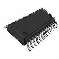
CY8CLED16P01-28PVXIT Cypress Semiconductor Corp, CY8CLED16P01-28PVXIT Datasheet - Page 26

CY8CLED16P01-28PVXIT
Manufacturer Part Number
CY8CLED16P01-28PVXIT
Description
IC PLC PSOC CMOS LED 16CH 28SSOP
Manufacturer
Cypress Semiconductor Corp
Series
PowerPSoC® CY8CLEDr
Datasheet
1.CY8CLED16P01-48LFXI.pdf
(46 pages)
Specifications of CY8CLED16P01-28PVXIT
Package / Case
28-SSOP
Core Processor
M8C
Core Size
8-Bit
Speed
24MHz
Connectivity
I²C, IrDA, SPI, UART/USART
Peripherals
LED, PLC, POR, PWM, WDT
Number Of I /o
24
Program Memory Size
32KB (32K x 8)
Program Memory Type
FLASH
Ram Size
2K x 8
Voltage - Supply (vcc/vdd)
4.75 V ~ 5.25 V
Data Converters
A/D 4x14b; D/A 4x9b
Oscillator Type
Internal
Operating Temperature
-40°C ~ 85°C
Operating Supply Voltage
4.75 V to 5.25 V
Maximum Supply Current
8 mA
Maximum Operating Temperature
+ 85 C
Mounting Style
SMD/SMT
Minimum Operating Temperature
- 40 C
Lead Free Status / RoHS Status
Lead free / RoHS Compliant
Eeprom Size
-
Lead Free Status / Rohs Status
Details
10.2 Operating Temperature
Table 10-3. Operating Temperature
10.3 DC Electrical Characteristics
10.3.1 DC Chip-Level Specifications
The following table lists guaranteed maximum and minimum specifications for the voltage and temperature ranges: 4.75V to 5.25V
and -40 ° C ≤ T
Table 10-4. DC Chip-Level Specifications
10.3.2 DC General Purpose IO Specifications
The following table lists guaranteed maximum and minimum specifications for the voltage and temperature range: 4.75V to 5.25V and
-40 ° C ≤ T
Table 10-5. DC GPIO Specifications
Document Number: 001-49263 Rev. *E
T
T
Vdd
I
V
R
R
V
V
I
I
V
V
V
I
C
C
DD
OH
OL
IL
Symbol
Symbol
Symbol
A
J
REF
OH
OL
IL
IH
H
PU
PD
IN
OUT
A
≤ 85 ° C. Typical parameters apply to 5V at 25 ° C and are for design guidance only.
Supply Voltage
Supply Current
Reference Voltage (Bandgap)
Pull Up Resistor
Pull Down Resistor
High Output Level
Low Output Level
High Level Source Current
Low Level Source Current
Input Low Level
Input High Level
Input Hysterisis
Input Leakage (Absolute Value)
Capacitive Load on Pins as Input
Capacitive Load on Pins as Output
Ambient Temperature
Junction Temperature
A
≤ 85 ° C. Typical parameters apply to 5V at 25 ° C and are for design guidance only.
Description
Description
Description
Min
-40
-40
4.75
1.28
Vdd -
Min
Min
1.0
2.1
10
25
–
4
4
–
–
–
–
–
–
Typ
Typ
1.3
–
–
Typ
5.6
5.6
3.5
3.5
–
8
60
–
–
–
–
–
1
–
+100
Max
+85
Max
5.25
1.32
14
Max
0.75
0.8
10
10
8
8
–
–
–
–
–
Units
Units
mA
Units
o
o
V
V
mA
mA
mV
C
C
k Ω
k Ω
nA
pF
pF
V
V
V
V
Conditions are 5.0V, T
CPU = 3 MHz, SYSCLK doubler disabled,
VC1 = 1.5 MHz, VC2 = 93.75 kHz,
VC3 = 0.366 kHz.
Trimmed for appropriate Vdd.
The temperature rise from ambient to
junction is package specific. See
Impedances
the power consumption to comply with this
requirement.
IOH = 10 mA, (8 total loads, 4 on even port
pins (for example, P0[2], P1[4]), 4 on odd
port pins (for example, P0[3], P1[5])). 80
mA maximum combined IOH budget.
IOL = 25 mA, (8 total loads, 4 on even port
pins (for example, P0[2], P1[4]), 4 on odd
port pins (for example, P0[3], P1[5])). 150
mA maximum combined IOL budget.
VOH = Vdd-1.0V, see the limitations of the
total current in the note for VOH
VOL = 0.75V, see the limitations of the total
current in the note for VOL
Gross tested to 1 μ A.
Package and pin dependent. Temp = 25°C.
Package and pin dependent. Temp = 25°C.
on page 41.The user must limit
CY8CLED16P01
Notes
Notes
Notes
A
= 25°C,
Page 26 of 46
Thermal
[+] Feedback
[+] Feedback


