MC9S08GT60ACFDE Freescale Semiconductor, MC9S08GT60ACFDE Datasheet - Page 114
MC9S08GT60ACFDE
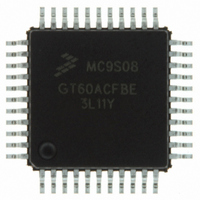
Manufacturer Part Number
MC9S08GT60ACFDE
Description
IC MCU 60K FLASH 4K RAM 48-QFN
Manufacturer
Freescale Semiconductor
Series
HCS08r
Datasheet
1.MC9S08GT60ACFDER.pdf
(302 pages)
Specifications of MC9S08GT60ACFDE
Core Processor
HCS08
Core Size
8-Bit
Speed
40MHz
Connectivity
I²C, SCI, SPI
Peripherals
LVD, POR, PWM, WDT
Number Of I /o
39
Program Memory Size
60KB (60K x 8)
Program Memory Type
FLASH
Ram Size
4K x 8
Voltage - Supply (vcc/vdd)
1.8 V ~ 3.6 V
Data Converters
A/D 8x10b
Oscillator Type
Internal
Operating Temperature
-40°C ~ 85°C
Package / Case
48-QFN
Processor Series
S08GT
Core
HCS08
Data Bus Width
8 bit
Data Ram Size
4 KB
Interface Type
SCI/SPI
Maximum Clock Frequency
40 MHz
Number Of Programmable I/os
39
Number Of Timers
2
Operating Supply Voltage
0 V to 1.8 V
Maximum Operating Temperature
+ 85 C
Mounting Style
SMD/SMT
3rd Party Development Tools
EWS08
Development Tools By Supplier
M68EVB908GB60E, M68DEMO908GB60E
Minimum Operating Temperature
- 40 C
On-chip Adc
8-ch x 10-bit
For Use With
M68DEMO908GB60E - BOARD DEMO MC9S08GB60M68EVB908GB60E - BOARD EVAL FOR MC9S08GB60
Lead Free Status / RoHS Status
Lead free / RoHS Compliant
Eeprom Size
-
Lead Free Status / Rohs Status
Lead free / RoHS Compliant
Available stocks
Company
Part Number
Manufacturer
Quantity
Price


Internal Clock Generator (S08ICGV2)
7.3.8
A clock mode is requested by writing to CLKS1:CLKS0 and the actual clock mode is indicated by
CLKST1:CLKST0. Provided minimum conditions are met, the status shown in CLKST1:CLKST0 should
be the same as the requested mode in CLKS1:CLKS0.
CLKST, and ICGOUT. It also shows the conditions for CLKS = CLKST or the reason CLKS ≠ CLKST.
114
1
2
3
(CLKST)
Actual
CLKST will not update immediately after a write to CLKS. Several bus cycles are required before CLKST updates to the new
value.
The reference frequency has no effect on ICGOUT in SCM, but the reference frequency is still used in making the comparisons
that determine the DCOS bit.
After initial LOCK; will be ICGDCLK/2R during initial locking process and while FLL is re-locking after the MFD bits are
changed.
Mode
SCM
(XX)
FBE
FEE
(00)
(01)
(10)
(11)
FEI
Off
Clock Mode Requirements
Desired
(CLKS)
Mode
SCM
(XX)
FBE
FBE
FEE
FEE
FBE
FEE
FEE
(10)
(00)
(01)
(10)
(11)
(01)
(11)
(10)
(11)
(11)
FEI
FEI
Off
If a crystal will be used before the next reset, then be sure to set REFS = 1
and CLKS = 1x on the first write to the ICGC1 register. Failure to do so will
result in “locking” REFS = 0, which will prevent the oscillator amplifier
from being enabled until the next reset occurs.
Range
X
X
X
X
X
X
X
X
0
0
0
1
(f
f
f
f
f
ICGIRCLK
ICGIRCLK
ICGIRCLK
Frequency
f
f
Reference
ICGIRCLK
REFERENCE
f
f
ICGIRCLK
ICGIRCLK
ICGERCLK
ICGERCLK
0
0
0
0
MC9S08GB60A Data Sheet, Rev. 2
/7
/7
/7
/7
Table 7-2. ICG State Table
/7
/7
(1)
(1)
(1)
2
)
128/f
Comparison
Cycle Time
2/f
8/f
8/f
8/f
8/f
8/f
8/f
NOTE
ICGERCLK
ICGIRCLK
ICGIRCLK
ICGIRCLK
ICGIRCLK
ICGIRCLK
ICGIRCLK
ICGERCLK
—
—
—
—
Table 7-2
ICGDCLK/R
ICGERCLK/R
ICGERCLK/R
ICGDCLK/R
ICGDCLK/R
ICGDCLK/R
ICGDCLK/R
ICGDCLK/R
ICGDCLK/R
ICGDCLK/R
ICGOUT
shows the relationship between CLKS,
0
0
(2)
3
Not switching from
Conditions
CLKS = CLKST
ERCS = 1 and
ERCS = 1 and
FBE to SCM
DCOS = 1
DCOS = 1
DCOS = 1
ERCS = 1
—
—
—
—
—
—
—
Freescale Semiconductor
1
for
DCOS = 0 or
LOCS = 1 &
ERCS = 0
DCOS = 0
ERCS = 0
ERCS = 0
ERCS = 0
ERCS = 1
CLKS1 =
Reason
CLKST
—
—
—
—
—
—
Related parts for MC9S08GT60ACFDE
Image
Part Number
Description
Manufacturer
Datasheet
Request
R

Part Number:
Description:
Manufacturer:
Freescale Semiconductor, Inc
Datasheet:
Part Number:
Description:
Manufacturer:
Freescale Semiconductor, Inc
Datasheet:
Part Number:
Description:
Manufacturer:
Freescale Semiconductor, Inc
Datasheet:
Part Number:
Description:
Manufacturer:
Freescale Semiconductor, Inc
Datasheet:
Part Number:
Description:
Manufacturer:
Freescale Semiconductor, Inc
Datasheet:
Part Number:
Description:
Manufacturer:
Freescale Semiconductor, Inc
Datasheet:
Part Number:
Description:
Manufacturer:
Freescale Semiconductor, Inc
Datasheet:
Part Number:
Description:
Manufacturer:
Freescale Semiconductor, Inc
Datasheet:
Part Number:
Description:
Manufacturer:
Freescale Semiconductor, Inc
Datasheet:
Part Number:
Description:
Manufacturer:
Freescale Semiconductor, Inc
Datasheet:
Part Number:
Description:
Manufacturer:
Freescale Semiconductor, Inc
Datasheet:
Part Number:
Description:
Manufacturer:
Freescale Semiconductor, Inc
Datasheet:
Part Number:
Description:
Manufacturer:
Freescale Semiconductor, Inc
Datasheet:
Part Number:
Description:
Manufacturer:
Freescale Semiconductor, Inc
Datasheet:
Part Number:
Description:
Manufacturer:
Freescale Semiconductor, Inc
Datasheet: