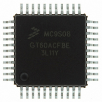
MC9S08GT60ACFDE Freescale Semiconductor, MC9S08GT60ACFDE Datasheet - Page 276

MC9S08GT60ACFDE
Manufacturer Part Number
MC9S08GT60ACFDE
Description
IC MCU 60K FLASH 4K RAM 48-QFN
Manufacturer
Freescale Semiconductor
Series
HCS08r
Datasheet
1.MC9S08GT60ACFDER.pdf
(302 pages)
Specifications of MC9S08GT60ACFDE
Core Processor
HCS08
Core Size
8-Bit
Speed
40MHz
Connectivity
I²C, SCI, SPI
Peripherals
LVD, POR, PWM, WDT
Number Of I /o
39
Program Memory Size
60KB (60K x 8)
Program Memory Type
FLASH
Ram Size
4K x 8
Voltage - Supply (vcc/vdd)
1.8 V ~ 3.6 V
Data Converters
A/D 8x10b
Oscillator Type
Internal
Operating Temperature
-40°C ~ 85°C
Package / Case
48-QFN
Processor Series
S08GT
Core
HCS08
Data Bus Width
8 bit
Data Ram Size
4 KB
Interface Type
SCI/SPI
Maximum Clock Frequency
40 MHz
Number Of Programmable I/os
39
Number Of Timers
2
Operating Supply Voltage
0 V to 1.8 V
Maximum Operating Temperature
+ 85 C
Mounting Style
SMD/SMT
3rd Party Development Tools
EWS08
Development Tools By Supplier
M68EVB908GB60E, M68DEMO908GB60E
Minimum Operating Temperature
- 40 C
On-chip Adc
8-ch x 10-bit
For Use With
M68DEMO908GB60E - BOARD DEMO MC9S08GB60M68EVB908GB60E - BOARD EVAL FOR MC9S08GB60
Lead Free Status / RoHS Status
Lead free / RoHS Compliant
Eeprom Size
-
Lead Free Status / Rohs Status
Lead free / RoHS Compliant
Available stocks
Company
Part Number
Manufacturer
Quantity
Price
- Current page: 276 of 302
- Download datasheet (8Mb)
Appendix A Electrical Characteristics
A.9.1
1
2
3
4
276
Bus frequency (t
Real-time interrupt internal oscillator period
External reset pulse width
Reset low drive
Active background debug mode latch setup time
Active background debug mode latch hold time
IRQ pulse width
Port rise and fall time (load = 50 pF)
This is the shortest pulse that is guaranteed to be recognized as a reset pin request. Shorter pulses are not guaranteed to
override reset requests from internal sources.
When any reset is initiated, internal circuitry drives the reset pin low for about 34 cycles of f
on the reset pin about 38 cycles later to distinguish external reset requests from internal requests.
This is the minimum pulse width that is guaranteed to pass through the pin synchronization circuitry. Shorter pulses may or
may not be recognized. In stop mode, the synchronizer is bypassed so shorter pulses can be recognized in that case.
Timing is shown with respect to 20% V
Slew rate control disabled
Slew rate control enabled
Control Timing
2
3
cyc
= 1/f
RESET PIN
Bus
Parameter
1
Figure A-12. Active Background Debug Mode Latch Timing
)
BKGD/MS
4
RESET
DD
and 80% V
MC9S08GB60A Data Sheet, Rev. 2
Table A-10. Control Timing
Figure A-11. Reset Timing
t
MSSU
DD
levels. Temperature range –40°C to 85°C.
t
Symbol
Rise
t
t
t
MSSU
t
rstdrv
t
f
extrst
t
MSH
t
ILIH
Bus
RTI
extrst
, t
Fall
f
f
1.5 x t
Self_reset
Self_reset
1.5 x
34 x
Min
700
dc
25
25
—
—
cyc
t
MSH
Self_reset
Typical
30
—
3
and then samples the level
Freescale Semiconductor
1300
Max
20
—
—
—
—
—
MHz
Unit
μs
ns
ns
ns
ns
ns
ns
Related parts for MC9S08GT60ACFDE
Image
Part Number
Description
Manufacturer
Datasheet
Request
R
Part Number:
Description:
Manufacturer:
Freescale Semiconductor, Inc
Datasheet:
Part Number:
Description:
Manufacturer:
Freescale Semiconductor, Inc
Datasheet:
Part Number:
Description:
Manufacturer:
Freescale Semiconductor, Inc
Datasheet:
Part Number:
Description:
Manufacturer:
Freescale Semiconductor, Inc
Datasheet:
Part Number:
Description:
Manufacturer:
Freescale Semiconductor, Inc
Datasheet:
Part Number:
Description:
Manufacturer:
Freescale Semiconductor, Inc
Datasheet:
Part Number:
Description:
Manufacturer:
Freescale Semiconductor, Inc
Datasheet:
Part Number:
Description:
Manufacturer:
Freescale Semiconductor, Inc
Datasheet:
Part Number:
Description:
Manufacturer:
Freescale Semiconductor, Inc
Datasheet:
Part Number:
Description:
Manufacturer:
Freescale Semiconductor, Inc
Datasheet:
Part Number:
Description:
Manufacturer:
Freescale Semiconductor, Inc
Datasheet:
Part Number:
Description:
Manufacturer:
Freescale Semiconductor, Inc
Datasheet:
Part Number:
Description:
Manufacturer:
Freescale Semiconductor, Inc
Datasheet:
Part Number:
Description:
Manufacturer:
Freescale Semiconductor, Inc
Datasheet:
Part Number:
Description:
Manufacturer:
Freescale Semiconductor, Inc
Datasheet:


