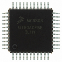
MC9S08GT60ACFDE Freescale Semiconductor, MC9S08GT60ACFDE Datasheet - Page 31

MC9S08GT60ACFDE
Manufacturer Part Number
MC9S08GT60ACFDE
Description
IC MCU 60K FLASH 4K RAM 48-QFN
Manufacturer
Freescale Semiconductor
Series
HCS08r
Datasheet
1.MC9S08GT60ACFDER.pdf
(302 pages)
Specifications of MC9S08GT60ACFDE
Core Processor
HCS08
Core Size
8-Bit
Speed
40MHz
Connectivity
I²C, SCI, SPI
Peripherals
LVD, POR, PWM, WDT
Number Of I /o
39
Program Memory Size
60KB (60K x 8)
Program Memory Type
FLASH
Ram Size
4K x 8
Voltage - Supply (vcc/vdd)
1.8 V ~ 3.6 V
Data Converters
A/D 8x10b
Oscillator Type
Internal
Operating Temperature
-40°C ~ 85°C
Package / Case
48-QFN
Processor Series
S08GT
Core
HCS08
Data Bus Width
8 bit
Data Ram Size
4 KB
Interface Type
SCI/SPI
Maximum Clock Frequency
40 MHz
Number Of Programmable I/os
39
Number Of Timers
2
Operating Supply Voltage
0 V to 1.8 V
Maximum Operating Temperature
+ 85 C
Mounting Style
SMD/SMT
3rd Party Development Tools
EWS08
Development Tools By Supplier
M68EVB908GB60E, M68DEMO908GB60E
Minimum Operating Temperature
- 40 C
On-chip Adc
8-ch x 10-bit
For Use With
M68DEMO908GB60E - BOARD DEMO MC9S08GB60M68EVB908GB60E - BOARD EVAL FOR MC9S08GB60
Lead Free Status / RoHS Status
Lead free / RoHS Compliant
Eeprom Size
-
Lead Free Status / Rohs Status
Lead free / RoHS Compliant
Available stocks
Company
Part Number
Manufacturer
Quantity
Price
- Current page: 31 of 302
- Download datasheet (8Mb)
For information about controlling these pins as general-purpose I/O pins, see
Input/Output.” For information about how and when on-chip peripheral systems use these pins, refer to the
appropriate section from
When an on-chip peripheral system is controlling a pin, data direction control bits still determine what is
read from port data registers even though the peripheral module controls the pin direction by controlling
the enable for the pin’s output buffer. See
Pullup enable bits for each input pin control whether on-chip pullup devices are enabled whenever the pin
is acting as an input even if it is being controlled by an on-chip peripheral module. When the PTA7–PTA4
pins are controlled by the KBI module and are configured for rising-edge/high-level sensitivity, the pullup
enable control bits enable pulldown devices rather than pullup devices. Similarly, when IRQ is configured
as the IRQ input and is set to detect rising edges, the pullup enable control bit enables a pulldown device
rather than a pullup device.
Freescale Semiconductor
1
PTA7–PTA0
PTB7–PTB0
PTC7–PTC4
PTC3–PTC2
PTC1–PTC0
PTD7–PTD3
PTD2–PTD0
PTE7–PTE6
PTE5
PTE4
PTE3
PTE2
PTE1–PTE0
PTF7–PTF0
PTG7–PTG3
PTG2–PTG1
PTG0
See this section for information about modules that share these pins.
Port Pins
KBI1P7–KBI1P0
AD1P7–AD1P0
SCL1–SDA1
RxD2–TxD2
TPM2CH4–
TPM1CH2–
SPSCK1
MISO1
MOSI1
SS1
RxD1–TxD1
EXTAL–XTAL
BKGD/MS
TPM2CH0
TPM1CH0
Alternate
Function
Table
—
—
—
—
2-1.
Table 2-1. Pin Sharing References
MC9S08GB60A Data Sheet, Rev. 2
Chapter 2, “Pins and Connections”
Chapter 14, “Analog-to-Digital Converter (S08ATDV3)”
Chapter 6, “Parallel Input/Output”
Chapter 13, “Inter-Integrated Circuit (S08IICV1)”
Chapter 11, “Serial Communications Interface (S08SCIV1)”
Chapter 10, “Timer/PWM (S08TPMV1)”
Chapter 10, “Timer/PWM (S08TPMV1)”
Chapter 6, “Parallel Input/Output”
Chapter 12, “Serial Peripheral Interface (S08SPIV3)”
Chapter 11, “Serial Communications Interface (S08SCIV1)”
Chapter 6, “Parallel Input/Output”
Chapter 6, “Parallel Input/Output”
Chapter 7, “Internal Clock Generator (S08ICGV2)”
Chapter 15, “Development Support”
Chapter 6, “Parallel
Input/Output” for details.
Reference
1
Chapter 6, “Parallel
Chapter 2 Pins and Connections
31
Related parts for MC9S08GT60ACFDE
Image
Part Number
Description
Manufacturer
Datasheet
Request
R
Part Number:
Description:
Manufacturer:
Freescale Semiconductor, Inc
Datasheet:
Part Number:
Description:
Manufacturer:
Freescale Semiconductor, Inc
Datasheet:
Part Number:
Description:
Manufacturer:
Freescale Semiconductor, Inc
Datasheet:
Part Number:
Description:
Manufacturer:
Freescale Semiconductor, Inc
Datasheet:
Part Number:
Description:
Manufacturer:
Freescale Semiconductor, Inc
Datasheet:
Part Number:
Description:
Manufacturer:
Freescale Semiconductor, Inc
Datasheet:
Part Number:
Description:
Manufacturer:
Freescale Semiconductor, Inc
Datasheet:
Part Number:
Description:
Manufacturer:
Freescale Semiconductor, Inc
Datasheet:
Part Number:
Description:
Manufacturer:
Freescale Semiconductor, Inc
Datasheet:
Part Number:
Description:
Manufacturer:
Freescale Semiconductor, Inc
Datasheet:
Part Number:
Description:
Manufacturer:
Freescale Semiconductor, Inc
Datasheet:
Part Number:
Description:
Manufacturer:
Freescale Semiconductor, Inc
Datasheet:
Part Number:
Description:
Manufacturer:
Freescale Semiconductor, Inc
Datasheet:
Part Number:
Description:
Manufacturer:
Freescale Semiconductor, Inc
Datasheet:
Part Number:
Description:
Manufacturer:
Freescale Semiconductor, Inc
Datasheet:


