MC9S12XA256CAL Freescale Semiconductor, MC9S12XA256CAL Datasheet - Page 1272
MC9S12XA256CAL
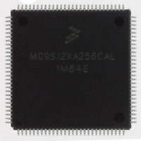
Manufacturer Part Number
MC9S12XA256CAL
Description
IC MCU 256K FLASH 112-LQFP
Manufacturer
Freescale Semiconductor
Series
HCS12r
Specifications of MC9S12XA256CAL
Core Processor
HCS12X
Core Size
16-Bit
Speed
80MHz
Connectivity
EBI/EMI, I²C, IrDA, LIN, SCI, SPI
Peripherals
LVD, POR, PWM, WDT
Number Of I /o
91
Program Memory Size
256KB (256K x 8)
Program Memory Type
FLASH
Eeprom Size
4K x 8
Ram Size
16K x 8
Voltage - Supply (vcc/vdd)
2.35 V ~ 5.5 V
Data Converters
A/D 16x10b
Oscillator Type
External
Operating Temperature
-40°C ~ 85°C
Package / Case
112-LQFP
No. Of I/o's
91
Eeprom Memory Size
4KB
Ram Memory Size
16KB
Cpu Speed
80MHz
No. Of Timers
1
No. Of Pwm Channels
8
Digital Ic Case Style
LQFP
Rohs Compliant
Yes
Processor Series
S12XA
Core
HCS12
Data Bus Width
16 bit
Data Ram Size
16 KB
Interface Type
CAN, I2C, SCI, SPI
Maximum Clock Frequency
40 MHz
Number Of Programmable I/os
91
Number Of Timers
12
Maximum Operating Temperature
+ 85 C
Mounting Style
SMD/SMT
3rd Party Development Tools
EWHCS12
Development Tools By Supplier
EVB9S12XDP512E
Minimum Operating Temperature
- 40 C
On-chip Adc
2 (10 bit, 16 Channel)
Package
112LQFP
Family Name
HCS12
Maximum Speed
40 MHz
Operating Supply Voltage
2.5|5 V
Lead Free Status / RoHS Status
Lead free / RoHS Compliant
Available stocks
Company
Part Number
Manufacturer
Quantity
Price
Company:

Part Number:
MC9S12XA256CAL
Manufacturer:
AD
Quantity:
101
Company:
Part Number:
MC9S12XA256CAL
Manufacturer:
Freescale Semiconductor
Quantity:
10 000
Part Number:
MC9S12XA256CAL
Manufacturer:
FREESCALE
Quantity:
20 000


Appendix A Electrical Characteristics
A.7
This section provides electrical parametrics and ratings for the SPI. In
conditions are listed.
1
A.7.1
In
In
1274
Drive mode
Load capacitance C
Thresholds for delay measurement points
Timing specified for equal load on all SPI output pins. Avoid asymmetric load.
Figure A-6
Figure A-7
(CPOL = 1)
(CPOL = 0)
(Output)
(Output)
(Output)
(Output)
1. If configured as an output.
2. LSBF = 0. For LSBF = 1, bit order is LSB, bit 1, ..., bit 6, MSB.
(Input)
MISO
MOSI
SCK
SCK
SS1
SPI Timing
Master Mode
the timing diagram for master mode with transmission format CPHA = 0 is depicted.
the timing diagram for master mode with transmission format CPHA=1 is depicted.
LOAD
1
,
on all outputs
2
5
10
MSB IN2
MSB OUT2
Description
6
Figure A-6. SPI Master Timing (CPHA = 0)
4
Table A-25. Measurement Conditions
MC9S12XDP512 Data Sheet, Rev. 2.21
1
4
Bit 6 . . . 1
Bit 6 . . . 1
9
12
12
LSB IN
LSB OUT
Table A-25
13
13
(20% / 80%) V
Full drive mode
Value
50
11
the measurement
Freescale Semiconductor
3
DDX
Unit
pF
—
V
Related parts for MC9S12XA256CAL
Image
Part Number
Description
Manufacturer
Datasheet
Request
R

Part Number:
Description:
Manufacturer:
Freescale Semiconductor, Inc
Datasheet:
Part Number:
Description:
Manufacturer:
Freescale Semiconductor, Inc
Datasheet:
Part Number:
Description:
Manufacturer:
Freescale Semiconductor, Inc
Datasheet:
Part Number:
Description:
Manufacturer:
Freescale Semiconductor, Inc
Datasheet:
Part Number:
Description:
Manufacturer:
Freescale Semiconductor, Inc
Datasheet:
Part Number:
Description:
Manufacturer:
Freescale Semiconductor, Inc
Datasheet:
Part Number:
Description:
Manufacturer:
Freescale Semiconductor, Inc
Datasheet:
Part Number:
Description:
Manufacturer:
Freescale Semiconductor, Inc
Datasheet:
Part Number:
Description:
Manufacturer:
Freescale Semiconductor, Inc
Datasheet:
Part Number:
Description:
Manufacturer:
Freescale Semiconductor, Inc
Datasheet:
Part Number:
Description:
Manufacturer:
Freescale Semiconductor, Inc
Datasheet:
Part Number:
Description:
Manufacturer:
Freescale Semiconductor, Inc
Datasheet:
Part Number:
Description:
Manufacturer:
Freescale Semiconductor, Inc
Datasheet:
Part Number:
Description:
Manufacturer:
Freescale Semiconductor, Inc
Datasheet:
Part Number:
Description:
Manufacturer:
Freescale Semiconductor, Inc
Datasheet: