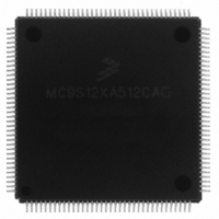
MC9S12XA512CAG Freescale Semiconductor, MC9S12XA512CAG Datasheet - Page 76

MC9S12XA512CAG
Manufacturer Part Number
MC9S12XA512CAG
Description
IC MCU 512K FLASH 144-LQFP
Manufacturer
Freescale Semiconductor
Series
HCS12r
Specifications of MC9S12XA512CAG
Core Processor
HCS12X
Core Size
16-Bit
Speed
80MHz
Connectivity
EBI/EMI, I²C, IrDA, LIN, SCI, SPI
Peripherals
LVD, POR, PWM, WDT
Number Of I /o
119
Program Memory Size
512KB (512K x 8)
Program Memory Type
FLASH
Eeprom Size
4K x 8
Ram Size
32K x 8
Voltage - Supply (vcc/vdd)
2.35 V ~ 5.5 V
Data Converters
A/D 24x10b
Oscillator Type
External
Operating Temperature
-40°C ~ 85°C
Package / Case
144-LQFP
Processor Series
S12XA
Core
HCS12
Data Bus Width
16 bit
Data Ram Size
32 KB
Interface Type
CAN, I2C, SCI, SPI
Maximum Clock Frequency
40 MHz
Number Of Programmable I/os
119
Number Of Timers
12
Maximum Operating Temperature
+ 85 C
Mounting Style
SMD/SMT
3rd Party Development Tools
EWHCS12
Development Tools By Supplier
EVB9S12XDP512E
Minimum Operating Temperature
- 40 C
On-chip Adc
2 (10 bit, 24 Channel)
Lead Free Status / RoHS Status
Lead free / RoHS Compliant
Available stocks
Company
Part Number
Manufacturer
Quantity
Price
Company:
Part Number:
MC9S12XA512CAG
Manufacturer:
Freescale
Quantity:
490
Company:
Part Number:
MC9S12XA512CAG
Manufacturer:
Freescale Semiconductor
Quantity:
10 000
- Current page: 76 of 1348
- Download datasheet (8Mb)
Chapter 1 Device Overview MC9S12XD-Family
1.6.2
When a reset occurs, MCU registers and control bits are changed to known start-up states. Refer to the
respective module Block Guides for register reset states.
1.6.2.1
Refer to the PIM Block Guide for reset configurations of all peripheral module ports.
1.6.2.2
The RAM array is not initialized out of reset.
1.7
The COP timeout rate bits CR[2:0] and the WCOP bit in the COPCTL register are loaded on rising edge
of RESET from the Flash control register FCTL ($0107) located in the Flash EEPROM block. See
Table 1-13
at global address $7FFF0E during the reset sequence
76
COP Configuration
and
Effects of Reset
I/O Pins
Memory
If the MCU is secured the COP timeout rate is always set to the longest
period (CR[2:0] = 111) after COP reset.
Table 1-14
for coding. The FCTL register is loaded from the Flash configuration field byte
FCTL Register
FCTL Register
NV[2:0] in
Table 1-13. Initial COP Rate Configuration
NV[3] in
Table 1-14. Initial WCOP Configuration
000
001
010
011
100
101
110
111
1
0
MC9S12XDP512 Data Sheet, Rev. 2.21
NOTE
COPCTL Register
COPCTL Register
CR[2:0] in
WCOP in
111
110
101
100
011
010
001
000
0
1
Freescale Semiconductor
Related parts for MC9S12XA512CAG
Image
Part Number
Description
Manufacturer
Datasheet
Request
R
Part Number:
Description:
Manufacturer:
Freescale Semiconductor, Inc
Datasheet:
Part Number:
Description:
Manufacturer:
Freescale Semiconductor, Inc
Datasheet:
Part Number:
Description:
Manufacturer:
Freescale Semiconductor, Inc
Datasheet:
Part Number:
Description:
Manufacturer:
Freescale Semiconductor, Inc
Datasheet:
Part Number:
Description:
Manufacturer:
Freescale Semiconductor, Inc
Datasheet:
Part Number:
Description:
Manufacturer:
Freescale Semiconductor, Inc
Datasheet:
Part Number:
Description:
Manufacturer:
Freescale Semiconductor, Inc
Datasheet:
Part Number:
Description:
Manufacturer:
Freescale Semiconductor, Inc
Datasheet:
Part Number:
Description:
Manufacturer:
Freescale Semiconductor, Inc
Datasheet:
Part Number:
Description:
Manufacturer:
Freescale Semiconductor, Inc
Datasheet:
Part Number:
Description:
Manufacturer:
Freescale Semiconductor, Inc
Datasheet:
Part Number:
Description:
Manufacturer:
Freescale Semiconductor, Inc
Datasheet:
Part Number:
Description:
Manufacturer:
Freescale Semiconductor, Inc
Datasheet:
Part Number:
Description:
Manufacturer:
Freescale Semiconductor, Inc
Datasheet:
Part Number:
Description:
Manufacturer:
Freescale Semiconductor, Inc
Datasheet:


