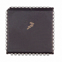
MC68HC711D3CFNE3 Freescale Semiconductor, MC68HC711D3CFNE3 Datasheet - Page 39

MC68HC711D3CFNE3
Manufacturer Part Number
MC68HC711D3CFNE3
Description
IC MCU 8BIT 2MHZ 44-PLCC
Manufacturer
Freescale Semiconductor
Series
HC11r
Specifications of MC68HC711D3CFNE3
Core Processor
HC11
Core Size
8-Bit
Speed
3MHz
Connectivity
SCI, SPI
Peripherals
POR, WDT
Number Of I /o
26
Program Memory Size
4KB (4K x 8)
Program Memory Type
OTP
Ram Size
192 x 8
Voltage - Supply (vcc/vdd)
4.5 V ~ 5.5 V
Oscillator Type
Internal
Operating Temperature
-40°C ~ 85°C
Package / Case
44-PLCC
Lead Free Status / RoHS Status
Lead free / RoHS Compliant
Eeprom Size
-
Data Converters
-
Available stocks
Company
Part Number
Manufacturer
Quantity
Price
Company:
Part Number:
MC68HC711D3CFNE3
Manufacturer:
SGS
Quantity:
6 218
Company:
Part Number:
MC68HC711D3CFNE3
Manufacturer:
Freescale Semiconductor
Quantity:
10 000
TECHNICAL DATA
$002C
$002D
$003C
$003D
$002B
$002E
$002F
$003A
$003B
$003E
$003F
$0030
$0038
$0039
The bootloader program is contained in the 192-byte bootstrap ROM. This ROM,
which appears as internal memory space at locations $BF40–$BFFF, is enabled only
if the MCU is reset in special bootstrap mode.
Memory locations are the same for expanded multiplexed and single-chip modes, ex-
cept for ROM in expanded mode and the bootloader ROM in special bootstrap mode.
The on-board 192-byte RAM is initially located at $0040 after reset, but can be placed
at any other 4K boundary ($x040) by writing an appropriate value to the INIT register.
The 4 Kbyte ROM is located at $F000 through $FFFF in all modes except expanded
multiplexed, in which it is located at $7000. ROM can be located at $F000 in expanded
multiplexed by entering single-chip mode out of reset and setting the MDA bit in the
HPRIO register to 1, thereby entering expanded mode from internal ROM. Disable
ROM by clearing the ROMON bit in the CONFIG register.
Hardware priority is built into RAM and I/O remapping. Registers and RAM have prior-
ity over ROM. In the event of conflicts, the higher priority resource takes precedence.
The 192 bytes of fully static RAM store instructions, variables, and temporary data.
The direct addressing mode can access RAM locations using a one-byte address op-
erand, saving program memory space and execution time, depending on the applica-
tion. RAM contents are preserved during periods of processor inactivity by two
methods, both of which reduce power consumption.
In the software-based STOP mode, the clocks are stopped while V
MCU. Because power supply current is directly related to operating frequency in
CMOS integrated circuits, only a very small amount of leakage exists when the clocks
are stopped.
to
RBOOT
TILOP
TDRE
R7/T7
RAM3
TCLR
Bit 7
Bit 7
Table 4-1 Register and Control Bit Assignments (Continued)
TIE
R8
0
0
SMOD
R6/T6
RAM2
TCIE
TC
T8
6
0
0
6
0
0
Freescale Semiconductor, Inc.
OPERATING MODES AND ON-CHIP MEMORY
For More Information On This Product,
OCCR
RDRF
RAM1
R5/T5
SCP1
IRQE
MDA
RIE
0
5
5
0
Go to: www.freescale.com
IRVNE
RAM0
R4/T4
CBYP
SCP0
IDLE
DLY
ILIE
M
4
4
0
PSEL3
WAKE
RCKB
R3/T3
REG3
DISR
CME
OR
TE
3
3
0
NOCOP
PSEL2
SCR2
R2/T2
REG2
FCM
RE
NF
2
0
0
2
ROMON
PSEL1
REG1
FCOP
SCR1
R1/T1
RWU
CR1
FE
1
0
1
PSEL0
R0/T0
REG0
SCR0
Bit 0
SBK
CR0
Bit 0
0
0
0
0
DD
powers the
Reserved
Reserved
Reserved
COPRST
OPTION
CONFIG
SCCR1
SCCR2
HPRIO
TEST1
SCDR
BAUD
SCSR
INIT
4-5


