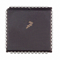
MC68HC711D3CFNE3 Freescale Semiconductor, MC68HC711D3CFNE3 Datasheet - Page 65

MC68HC711D3CFNE3
Manufacturer Part Number
MC68HC711D3CFNE3
Description
IC MCU 8BIT 2MHZ 44-PLCC
Manufacturer
Freescale Semiconductor
Series
HC11r
Specifications of MC68HC711D3CFNE3
Core Processor
HC11
Core Size
8-Bit
Speed
3MHz
Connectivity
SCI, SPI
Peripherals
POR, WDT
Number Of I /o
26
Program Memory Size
4KB (4K x 8)
Program Memory Type
OTP
Ram Size
192 x 8
Voltage - Supply (vcc/vdd)
4.5 V ~ 5.5 V
Oscillator Type
Internal
Operating Temperature
-40°C ~ 85°C
Package / Case
44-PLCC
Lead Free Status / RoHS Status
Lead free / RoHS Compliant
Eeprom Size
-
Data Converters
-
Available stocks
Company
Part Number
Manufacturer
Quantity
Price
Company:
Part Number:
MC68HC711D3CFNE3
Manufacturer:
SGS
Quantity:
6 218
Company:
Part Number:
MC68HC711D3CFNE3
Manufacturer:
Freescale Semiconductor
Quantity:
10 000
PORTD — Port D Data
DDRD — Data Direction Register for Port D
PACTL — Pulse Accumulator Control
DDD[7:0] — Data Direction for Port D
DDRA7 — Data Direction Control for Port A Bit 7
PAEN — Pulse Accumulator System Enable
PAMOD — Pulse Accumulator Mode
PEDGE — Pulse Accumulator Edge Control
DDRA3 — Data Direction for Port A Bit 3
TECHNICAL DATA
Alt. Func.:
RESET:
RESET:
RESET:
When port D is a general-purpose I/O port, the DDRD register controls the direction of
the I/O pins as follows:
In expanded and test modes, bits 6 and 7 are dedicated AS and R/W outputs.
When port D is functioning with the SPI system enabled, bit 5 is dedicated as the slave
select (SS) input. In SPI slave mode, DDD5 has no meaning or effect. In SPI master
mode, DDD5 affects port D bit 5 as follows:
If the SPI is enabled and expects port D bits 2, 3, and 4 (MISO, MOSI, and SCK) to be
inputs, then they are inputs, regardless of the state of DDRD bits 2, 3, and 4. If the SPI
expects port D bits 2, 3, and 4 to be outputs, they are outputs only if DDRD bits 2, 3,
and 4 are set.
Refer to SECTION 9 TIMING SYSTEM.
Refer to SECTION 9 TIMING SYSTEM.
Refer to SECTION 9 TIMING SYSTEM.
Refer to SECTION 9 TIMING SYSTEM.
Overridden if an output compare function is configured to control the PA3 pin.
0 = Configures the corresponding port D pin for input
1 = Configures the corresponding port D pin for output
0 = Port D bit 5 is an error-detect input to the SPI.
1 = Port D bit 5 is configured as a general-purpose output line.
0 = Input only
1 = Output
DDRA7
DDD7
Bit 7
PD7
R/W
Bit 7
Bit 7
0
0
0
DDD6
PAEN
PD6
AS
Freescale Semiconductor, Inc.
6
0
6
0
6
0
For More Information On This Product,
PAMOD
DDD5
PD5
Go to: www.freescale.com
5
0
5
0
5
0
PARALLEL I/O
PEDGE
DDD4
SCK
PD4
4
0
4
0
4
0
DDRA3
DDD3
MOSI
PD3
3
0
3
0
3
0
DDD2
MISO
I4/O5
PD2
2
0
2
0
2
0
DDD1
RTR1
PD1
TxD
1
0
1
0
1
0
$0008
$0009
$0026
DDD0
RTR0
Bit 0
Bit 0
Bit 0
PD0
RxD
0
0
0
6-3


