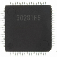
M30281F6HP#U5B Renesas Electronics America, M30281F6HP#U5B Datasheet - Page 191

M30281F6HP#U5B
Manufacturer Part Number
M30281F6HP#U5B
Description
IC M16C/28 MCU FLASH 48K 64LQFP
Manufacturer
Renesas Electronics America
Series
M16C™ M16C/Tiny/28r
Datasheet
1.M30280F6HPU9.pdf
(425 pages)
Specifications of M30281F6HP#U5B
Core Processor
M16C/60
Core Size
16-Bit
Speed
20MHz
Connectivity
I²C, IEBus, SIO, UART/USART
Peripherals
DMA, POR, PWM, Voltage Detect, WDT
Number Of I /o
55
Program Memory Size
48KB (48K x 8)
Program Memory Type
FLASH
Ram Size
4K x 8
Voltage - Supply (vcc/vdd)
2.7 V ~ 5.5 V
Data Converters
A/D 13x10b
Oscillator Type
Internal
Operating Temperature
-20°C ~ 85°C
Package / Case
64-LQFP
For Use With
R0K330290S000BE - KIT EVAL STARTER FOR M16C/29M30290T2-CPE - EMULATOR COMPACT M16C/26A/28/29M30290T2-CPE-HP - EMULATOR COMPACT FOR M16C/TINY
Lead Free Status / RoHS Status
Lead free / RoHS Compliant
Eeprom Size
-
Available stocks
Company
Part Number
Manufacturer
Quantity
Price
Part Number:
M30281F6HP#U5BM30281F6HP#D5
Manufacturer:
Renesas Electronics America
Quantity:
10 000
Part Number:
M30281F6HP#U5BM30281F6HP#U3
Manufacturer:
Renesas Electronics America
Quantity:
10 000
- Current page: 191 of 425
- Download datasheet (4Mb)
M
R
R
1
e
E
Figure 14.4 U0TB to U2TB, U0RB to U2RB, U0BRG to U2BRG Registers
. v
6
J
0
C
2
9
2 /
0 .
B
8
(b15)
NOTES:
NOTES:
0
b7
0
NOTES:
UARTi Receive Buffer Register (i=0 to 2)
UARTi Transmit Buffer Register (i=0 to 2)
b7
(b15)
b7
UARTi Baud Rate Generation Register (i=0 to 2)
0
1. When the SMD2 to SMD0 bits in the UiMR register are set to “000
2. The ABT bit is set to “0” by setting to “0” by program. (Writing “1” has no effect.)
G
1. Write to this register while serial I/O is neither transmitting nor receiving.
2. Use MOV instruction to write to this register.
3. Set the UiBRG register after setting the CLK1 and CLK0 bits in the UiC0 registers.
1. Use MOV instruction to write to this register.
4
J
disabled), all of the SUM, PER, FER and OER bits are set to “0” (no error). The SUM bit is set to “0” (no error) when all of the PER, FER and OER
bits are set to “0” (no error). Also, the PER and FER bits are set to “0” by reading the lower byte of the UiRB register.
Nothing is assigned at the bit 11 in the U0RB and U1RB registers. When write, set to "0". When read, its content is "0".
7
a
o r
The transfer clock is shown below when the setting value in the UiBRG register is set as n.
0 -
. n
(1) When the CKDIR bit in the UiMR register to “0” (internal clock)
(2) When the CKDIR bit in the UiMR register to “1” (external clock)
u
2
p
3
0
, 1
0
(
M
2
• Clock synchronous serial I/O mode
• Clock asynchronous serial I/O (UART) mode
• Clock synchronous serial I/O mode
• Clock asynchronous serial I/O (UART) mode
1
0
0
6
7
C
(b8)
(b8)
2 /
b0
b0
b0
, 8
page 169
b7
b7
M
1
6
C
2 /
f o
8
3
) B
8
(b10-b9)
Symbol
(b7-b0)
5
Assuming that set value = n, UiBRG divides the count source
by n + 1
Transmit data
Nothing is assigned.
When write, set to "0". When read, its content is indeterminate.
OER
FER
PER
SUM
ABT
(b8)
Bit
b0
b0
(1)
Arbitration lost detecting
flag
Overrun error flag
Framing error flag
Parity error flag
Error sum flag
Nothing is assigned.
When write, set to "0". When read, its content is indeterminate.
Symbol
U0TB
U1TB
U2TB
U0RB
Symbol
U1RB
U2RB
Symbol
U0BRG
U1BRG
U2BRG
(2)
(1, 2, 3)
: fj/(2(n+1))
: fj/(16(n+1))
: f
: f
EXT
EXT
Bit Name
2
/(16(n+1))
” (serial I/O disabled) or the RE bit in the UiC1 register is set to “0” (reception
(1)
Address
03A7
03AF
037F
(1)
fj : f1SIO, f2SIO, f8SIO, f32SIO
f
Address
03A3
03AB
037B
EXT
Function
(1)
(1)
Address
03A1
03A9
0379
: Input from CLKi pin
16
16
16
16
16
16
-03A6
-037E
-03A2
-037A
-03AE
-03AA
16
16
16
0 : Not detected
1 : Detected
0 : No overrun error
1 : Overrun error found
Receive data (D
Receive data (D
0 : No framing error
1 : Framing error found
0 : No parity error
1 : Parity error found
0 : No error
1 : Error found
16
16
16
16
16
16
Function
After Reset
Indeterminate
Indeterminate
Indeterminate
After Reset
Indeterminate
Indeterminate
Indeterminate
After Reset
Indeterminate
Indeterminate
Indeterminate
7
8
)
to D
0
)
Function
Setting Range
00
16
to FF
16
14. Serial I/O
RW
RW
RW
RO
RO
RO
RO
WO
RO
RO
RW
WO
Related parts for M30281F6HP#U5B
Image
Part Number
Description
Manufacturer
Datasheet
Request
R

Part Number:
Description:
KIT STARTER FOR M16C/29
Manufacturer:
Renesas Electronics America
Datasheet:

Part Number:
Description:
KIT STARTER FOR R8C/2D
Manufacturer:
Renesas Electronics America
Datasheet:

Part Number:
Description:
R0K33062P STARTER KIT
Manufacturer:
Renesas Electronics America
Datasheet:

Part Number:
Description:
KIT STARTER FOR R8C/23 E8A
Manufacturer:
Renesas Electronics America
Datasheet:

Part Number:
Description:
KIT STARTER FOR R8C/25
Manufacturer:
Renesas Electronics America
Datasheet:

Part Number:
Description:
KIT STARTER H8S2456 SHARPE DSPLY
Manufacturer:
Renesas Electronics America
Datasheet:

Part Number:
Description:
KIT STARTER FOR R8C38C
Manufacturer:
Renesas Electronics America
Datasheet:

Part Number:
Description:
KIT STARTER FOR R8C35C
Manufacturer:
Renesas Electronics America
Datasheet:

Part Number:
Description:
KIT STARTER FOR R8CL3AC+LCD APPS
Manufacturer:
Renesas Electronics America
Datasheet:

Part Number:
Description:
KIT STARTER FOR RX610
Manufacturer:
Renesas Electronics America
Datasheet:

Part Number:
Description:
KIT STARTER FOR R32C/118
Manufacturer:
Renesas Electronics America
Datasheet:

Part Number:
Description:
KIT DEV RSK-R8C/26-29
Manufacturer:
Renesas Electronics America
Datasheet:

Part Number:
Description:
KIT STARTER FOR SH7124
Manufacturer:
Renesas Electronics America
Datasheet:

Part Number:
Description:
KIT STARTER FOR H8SX/1622
Manufacturer:
Renesas Electronics America
Datasheet:

Part Number:
Description:
KIT DEV FOR SH7203
Manufacturer:
Renesas Electronics America
Datasheet:


