M30281F6HP#U5B Renesas Electronics America, M30281F6HP#U5B Datasheet - Page 288
M30281F6HP#U5B
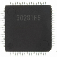
Manufacturer Part Number
M30281F6HP#U5B
Description
IC M16C/28 MCU FLASH 48K 64LQFP
Manufacturer
Renesas Electronics America
Series
M16C™ M16C/Tiny/28r
Datasheet
1.M30280F6HPU9.pdf
(425 pages)
Specifications of M30281F6HP#U5B
Core Processor
M16C/60
Core Size
16-Bit
Speed
20MHz
Connectivity
I²C, IEBus, SIO, UART/USART
Peripherals
DMA, POR, PWM, Voltage Detect, WDT
Number Of I /o
55
Program Memory Size
48KB (48K x 8)
Program Memory Type
FLASH
Ram Size
4K x 8
Voltage - Supply (vcc/vdd)
2.7 V ~ 5.5 V
Data Converters
A/D 13x10b
Oscillator Type
Internal
Operating Temperature
-20°C ~ 85°C
Package / Case
64-LQFP
For Use With
R0K330290S000BE - KIT EVAL STARTER FOR M16C/29M30290T2-CPE - EMULATOR COMPACT M16C/26A/28/29M30290T2-CPE-HP - EMULATOR COMPACT FOR M16C/TINY
Lead Free Status / RoHS Status
Lead free / RoHS Compliant
Eeprom Size
-
Available stocks
Company
Part Number
Manufacturer
Quantity
Price

Part Number:
M30281F6HP#U5BM30281F6HP#D5
Manufacturer:
Renesas Electronics America
Quantity:
10 000
Part Number:
M30281F6HP#U5BM30281F6HP#U3
Manufacturer:
Renesas Electronics America
Quantity:
10 000


R
R
M
e
E
1
. v
J
6
0
16.5.7 Bit 6: Communication Mode Select Bit (Transfer Direction Select Bit: TRX)
16.5.8 Bit 7: Communication mode select bit (master/slave select bit: MST)
C
2
9
This TRX bit decides a transfer direction for data communication. When the TRX bit is set to “0”, receive
mode is entered and data is received from a transmit device. When the TRX bit is set to “1”, transmit
mode is entered, and address data and control data are output to the SDA
generated in the SCL
The TRX bit is set to “1” automatically in the following condition:
The TRX bit is set to “0” in one of the following conditions:
The MST bit selects either master mode or slave mode for data communication. When the MST bit is set
to "0", slave mode is entered and the START/STOP condition generated by a master device are received.
The data communication is synchronized with the clock generted by the master. When the MST bit is set
to "1", master mode is entered and the START/STOP condition is generated.
Additionally, clocks required for the data communication are generated on the SCL
The MST bit is set to “0” in one of the following conditions.
0 .
B
2 /
•In slave mode, when the ALS in the S1D0 register to "0"(addressing format), the AAS flag is set to
•When an arbitration lost is detected
•When a STOP condition is detected
•When a START condition is detected
•When a START condition is disabled by the START condition duplicate protect function
•When the MST bit in the S10 register is set to "0"(slave mode) and a start condition is detected
•When the MST bit is set to "0" and the ACK non-return is detected
•When the ES0 bit is set to "0"(I
•When the IHR bit in the S1D0 register is set to "1"(reset)
0
0
“1”(address match) after the address data is received, and the received R/W bit is set to “1”
8
0
NOTES:
•After 1-byte data of a master whose arbtration is lost if arbitration lost is detected
•When a STOP condition is detected
•When a START condition is detected
•When a start condition is disabled by the START condition duplicate protect function
•When the IHR bit in the S1D0 register is set to "1"(reset)
•When the ES0 bit is set to "0"(I
4
J
G
7
a
1. START condition duplicate protect function:
o r
0 -
. n
u
set to "0" (bus free), all the MST, TRX and BB flags are set to "1" at the same time. However, if the
BB flag is set to "1" immediately after the BB flag setting is confirmed because a START condition
is generated by other master device, the MST and TRX bits cannot be written. The duplicate
protect function is valid from the rising edge of the BB flag until slave address is received. Refer
to 16.9 START Condition Generation Method for details.
2
When the START condition is generated, after confirming that the BB flag in the S1D0 register is
3
0
p
, 1
0
(
M
2
0
1
0
6
7
C
2 /
page 266
, 8
MM
M
1
.
6
C
f o
2 /
8
3
) B
8
5
2
C bus interface disabled)
2
C bus interface disabled)
16. MULTI-MASTER I
MM,
___
synchronized with a clock
MM
.
2
C bus INTERFACE
(1)
(1)
Related parts for M30281F6HP#U5B
Image
Part Number
Description
Manufacturer
Datasheet
Request
R

Part Number:
Description:
KIT STARTER FOR M16C/29
Manufacturer:
Renesas Electronics America
Datasheet:

Part Number:
Description:
KIT STARTER FOR R8C/2D
Manufacturer:
Renesas Electronics America
Datasheet:

Part Number:
Description:
R0K33062P STARTER KIT
Manufacturer:
Renesas Electronics America
Datasheet:

Part Number:
Description:
KIT STARTER FOR R8C/23 E8A
Manufacturer:
Renesas Electronics America
Datasheet:

Part Number:
Description:
KIT STARTER FOR R8C/25
Manufacturer:
Renesas Electronics America
Datasheet:

Part Number:
Description:
KIT STARTER H8S2456 SHARPE DSPLY
Manufacturer:
Renesas Electronics America
Datasheet:

Part Number:
Description:
KIT STARTER FOR R8C38C
Manufacturer:
Renesas Electronics America
Datasheet:

Part Number:
Description:
KIT STARTER FOR R8C35C
Manufacturer:
Renesas Electronics America
Datasheet:

Part Number:
Description:
KIT STARTER FOR R8CL3AC+LCD APPS
Manufacturer:
Renesas Electronics America
Datasheet:
Part Number:
Description:
KIT STARTER FOR RX610
Manufacturer:
Renesas Electronics America
Datasheet:

Part Number:
Description:
KIT STARTER FOR R32C/118
Manufacturer:
Renesas Electronics America
Datasheet:

Part Number:
Description:
KIT DEV RSK-R8C/26-29
Manufacturer:
Renesas Electronics America
Datasheet:

Part Number:
Description:
KIT STARTER FOR SH7124
Manufacturer:
Renesas Electronics America
Datasheet:

Part Number:
Description:
KIT STARTER FOR H8SX/1622
Manufacturer:
Renesas Electronics America
Datasheet:

Part Number:
Description:
KIT DEV FOR SH7203
Manufacturer:
Renesas Electronics America
Datasheet: