M38227ECFP Renesas Electronics America, M38227ECFP Datasheet
M38227ECFP
Specifications of M38227ECFP
Available stocks


Related parts for M38227ECFP


M38227ECFP Summary of contents
Page 1
To our customers, Old Company Name in Catalogs and Other Documents st On April 1 , 2010, NEC Electronics Corporation merged with Renesas Technology Corporation, and Renesas Electronics Corporation took over all the business of both companies. Therefore, although the ...
Page 2
All information included in this document is current as of the date this document is issued. Such information, however, is subject to change without any prior notice. Before purchasing or using any Renesas Electronics products listed herein, please confirm ...
Page 3
To all our customers Regarding the change of names mentioned in the document, such as Mitsubishi Electric and Mitsubishi XX, to Renesas Technology Corp. The semiconductor operations of Hitachi and Mitsubishi Electric were transferred to Renesas Technology Corporation on April ...
Page 4
DESCRIPTION The 3822 group is the 8-bit microcomputer based on the 740 fam- ily core technology. The 3822 group has the LCD drive control circuit, an 8-channel A-D converter, and a serial I/O as additional functions. The various microcomputers in ...
Page 5
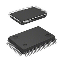
PIN CONFIGURATION (TOP VIEW) 61 SEG SEG 68 2 SEG SEG ...
Page 6
Fig. 3 Functional block diagram MITSUBISHI MICROCOMPUTERS 3822 Group SINGLE-CHIP 8-BIT CMOS MICROCOMPUTER ...
Page 7
PIN DESCRIPTION Table 1 Pin description (1) Pin Name Power source •Apply voltage of power source mended operating conditions”). V Analog refer- •Reference voltage input pin for A-D converter. REF ence voltage AV ...
Page 8
Table 2 Pin description (2) Pin Name Input port P4 P4 •1-bit Input port. 0 •CMOS compatible input level I/O port P4 •7-bit I/O port. 1 •CMOS compatible input level. P4 /INT , /INT 3 ...
Page 9
PART NUMBERING Product M3822 Fig. 4 Part numbering 6 H XXX FP Package type FP : 80P6N-A package GP : 80P6S-A package HP : 80P6Q-A package FS : 80D0 package ROM number Omitted in One Time PROM ...
Page 10
... M38222M2-XXXHP M38223M4-XXXFP M38223E4FP 16384 M38223M4-XXXGP (16254) M38223E4GP M38223M4-XXXHP M38223E4HP M38223E4FS M38227ECFP 49152 M38227ECHP (49022) M38227ECFS SINGLE-CHIP 8-BIT CMOS MICROCOMPUTER Memory Size ROM size ............................................................. bytes RAM size ............................................................ 384 to 1024 bytes Package 80P6N-A .................................... 0.8 mm-pitch plastic molded QFP 80P6S-A .................................. 0.65 mm-pitch plastic molded QFP 80P6Q-A ...
Page 11
GROUP EXPANSION (EXTENDED OPERATING TEMPERATURE VERSION) Mitsubishi plans to expand the 3822 group (extended operating temperature version) as follows: Memory Type Support for Mask ROM version. Memory Size ROM size ........................................................................ 48 K bytes RAM size ....................................................................... 1024 bytes Memory ...
Page 12
GROUP EXPANSION (M VERSION) Mitsubishi plans to expand the 3822 group (M version) as follows: Memory Type Support for Mask ROM version. Memory Size ROM size ........................................................... bytes RAM size .............................................................. 512 to 640 bytes ...
Page 13
GROUP EXPANSION (H VERSION) Mitsubishi plans to expand the 3822 group (H version) as follows: Memory Type Support for Mask ROM version. Memory Size ROM size ........................................................... bytes RAM size ............................................................ 512 to 1024 bytes ...
Page 14
FUNCTIONAL DESCRIPTION CENTRAL PROCESSING UNIT (CPU) The 3822 group uses the standard 740 family instruction set. Re- fer to the table of 740 family addressing modes and machine instructions or the 740 Family Software Manual for details on the instruction ...
Page 15
Interrupt request – ...
Page 16
The processor status register is an 8-bit register consisting of 5 flags which indicate the status of the processor after an arithmetic operation and 3 flags which decide MCU operation. Branch opera- tions can be performed ...
Page 17
Mode Register (CPUM)] 003B The CPU mode register contains the stack page selection bit and the internal system clock selection bit. The CPU mode register is allocated at address 003B b7 Fig. 11 Structure of CPU mode register 14 ...
Page 18
MEMORY Special Function Register (SFR) Area The Special Function Register area in the zero page contains con- trol registers such as I/O ports and timers. RAM RAM is used for data storage and for stack area of subroutine calls and ...
Page 19
Port P0 (P0) 16 0001 Port P0 direction register (P0D) 16 0002 Port P1 (P1) 16 Port P1 output control register (P1D) 0003 16 0004 Port P2 (P2) 16 Port P2 direction register (P2D) 0005 16 Port P3 (P3) ...
Page 20
I/O PORTS Direction Registers (ports P2, P4 P5-P7) The 3822 group has 49 programmable I/O pins arranged in seven I/O ports (ports P0–P2, P4 –P4 and P5-P7). The I/O ports P2 –P4 and P5-P7 have direction registers ...
Page 21
Table 9 List of I/O port function Name Input/Output Pin P0 /SEG – Port P0 Input/output /SEG individual ports /SEG – Port /SEG 7 31 Input/output, P2 – ...
Page 22
Ports P0 Segment output enable bit (Note) Direction register Data bus Port latch Pull-down control Segment output enable bit Note: Bit 0 of direction register. (3) Ports P3 –P3 4 ...
Page 23
Port P-channel output disable bit 5 x Serial I/O enable bit Transmit enable bit Direction register Data bus Port latch Serial I/O output (9) Port P4 7 Serial I/O mode selection bit Serial I/O ...
Page 24
...
Page 25
INTERRUPTS Interrupts occur by seventeen sources: eight external, eight inter- nal, and one software. Interrupt Control Each interrupt is controlled by an interrupt request bit, an interrupt enable bit, and the interrupt disable flag except for the software interrupt set ...
Page 26
Interrupt request bit Interrupt enable bit Interrupt disable flag (I) Fig. 18 Interrupt control b7 b0 Interrupt edge selection register (INTEDGE : address 003A INT interrupt edge selection bit 0 INT interrupt edge selection bit 1 INT interrupt edge selection ...
Page 27
Key Input Interrupt (Key-on wake-up) A Key-on wake-up interrupt request is generated by applying a falling edge to any pin of port P2 that have been set to input mode. In other words generated when AND of input ...
Page 28
TIMERS The 3822 group has five timers: timer X, timer Y, timer 1, timer 2, and timer 3. Timer X and timer Y are 16-bit timers, and timer 1, timer 2, and timer 3 are 8-bit timers. All timers are ...
Page 29
Timer X Timer 16-bit timer that can be selected in one of four modes and can be controlled the timer X write and the real time port by setting the timer X mode register. (1) Timer Mode ...
Page 30
Timer Y Timer 16-bit timer that can be selected in one of four modes. (1) Timer Mode The timer counts f(X )/16 (or f(X )/16 in low-speed mode). IN CIN (2) Period Measurement Mode CNTR interrupt request ...
Page 31
Timer 1, Timer 2, Timer 3 Timer 1, timer 2, and timer 3 are 8-bit timers. The count source for each timer can be selected by timer 123 mode register. The timer latch value is not affected by a change ...
Page 32
SERIAL I/O Serial I/O can be used as either clock synchronous or asynchro- nous (UART) serial I/O. A dedicated timer (baud rate generator) is also provided for baud rate generation ...
Page 33
Asynchronous Serial I/O (UART) Mode Clock asynchronous serial I/O mode (UART) can be selected by clearing the serial I/O mode selection bit of the serial I/O control register to “0”. Eight serial data transfer formats can be selected, and ...
Page 34
Buffer/Receive Buffer Register (TB/RB)] 0018 16 The transmit buffer register and the receive buffer register are lo- cated at the same address. The transmit buffer register is write-only and the receive buffer register is read-only charac- ter ...
Page 35
Serial I/O status register (SIOSTS : address 0019 ) ...
Page 36
A-D CONVERTER [A-D Conversion Register (AD)] 0035 The A-D conversion register is a read-only register that contains the result of an A-D conversion. When reading this register during an A-D conversion, the previous conversion result is read. [A-D Control Register ...
Page 37
LCD DRIVE CONTROL CIRCUIT The 3822 group has the built-in Liquid Crystal Display (LCD) drive control circuit consisting of the following. LCD display RAM Segment output enable register LCD mode register Selector Timing controller Common driver Segment driver Bias control ...
Page 38
Fig. 33 Block diagram of LCD controller/driver MITSUBISHI MICROCOMPUTERS 3822 Group SINGLE-CHIP 8-BIT CMOS MICROCOMPUTER 35 ...
Page 39
Bias Control and Applied Voltage to LCD Power Input Pins To the LCD power input pins (V –V ), apply the voltage shown Table 12 according to the bias value. Select a bias value by the bias ...
Page 40
LCD Display RAM Address 0040 to 004F is the designated RAM for the LCD dis play. When “1” are written to these addresses, the corresponding segments of the LCD display panel are turned on ...
Page 41
...
Page 42
1/4 duty ...
Page 43
CLOCK SYSTEM OUTPUT FUNCTION The internal system clock can be output from port P4 the output control register. Set bit 1 of the port P4 direction reg- ister to “1” when outputting clock Fig. 38 Structure of output ...
Page 44
RESET CIRCUIT To reset the microcomputer, RESET pin should be held at an “L” level for 2 µs or more. Then the RESET pin is returned to an “H” level (the power source voltage should be between V 5.5 V, ...
Page 45
...
Page 46
CLOCK GENERATING CIRCUIT The 3822 group has two built-in oscillation circuits. An oscillation circuit can be formed by connecting a resonator between and X ). Use the circuit constants in accordance OUT CIN COUT with the resonator ...
Page 47
“ 1 ” “0” Middle-/High-speed mode Main clock stop bit STP instruction Reset ...
Page 48
Reset “1” ...
Page 49
NOTES ON PROGRAMMING Processor Status Register The contents of the processor status register (PS) after a reset are undefined, except for the interrupt disable flag (I) which is “1”. Af- ter a reset, initialize flags which affect program execution. In ...
Page 50
NOTES ON USE Countermeasures against noise (1) Shortest wiring length Wiring for RESET pin Make the length of wiring which is connected to the RESET pin as short as possible. Especially, connect a capacitor across the RESET pin and the ...
Page 51
Oscillator concerns In order to obtain the stabilized operation clock on the user system and its condition, contact the oscillator manufacturer and select the oscillator and oscillation circuit constants. Be careful espe- cially when range of votage and temperature ...
Page 52
DATA REQUIRED FOR MASK ORDERS The following are necessary when ordering a mask ROM produc- tion: 1.Mask ROM Order Confirmation Form 2.Mark Specification Form 3.Data to be written to ROM, in EPROM form (three identical cop- ies) or one floppy ...
Page 53
Table 15 Absolute maximum ratings (Standard, One Time PROM version) Symbol Parameter V Power source voltage CC V Input voltage P0 – – – ...
Page 54
Table 17 Recommended operating conditions (Standard, One Time PROM version 2 – °C, unless otherwise noted) CC Symbol “H” total peak output current I OH(peak) “H” total peak output current I ...
Page 55
Table 18 Electrical characteristics (Standard, One Time PROM version) (V =4 –20 to 85°C, unless otherwise noted) CC Symbol Parameter “H” output voltage – – “H” ...
Page 56
Table 19 Electrical characteristics (Standard, One Time PROM version 2 – °C, unless otherwise noted) CC Symbol Parameter V RAM retention voltage RAM I Power source current CC Table 20 A-D ...
Page 57
Table 21 Timing requirements 1 (Standard, One Time PROM version 4 – °C, unless otherwise noted Symbol t Reset input “L” pulse width w(RESET) t ...
Page 58
Table 23 Switching characteristics 1 (Standard, One Time PROM version 4 – °C, unless otherwise noted Symbol t Serial I/O clock output “H” pulse width ...
Page 59
Table 25 Absolute maximum ratings (Extended operating temperature version) Symbol Parameter V Power source voltage CC V Input voltage P0 – – – Input voltage ...
Page 60
Table 27 Recommended operating conditions (Extended operating temperature version 2 – °C, and V CC Symbol “H” total peak output current I OH(peak) “H” total peak output current I OH(peak) “L” ...
Page 61
Table 28 Electrical characteristics (Extended operating temperature version) (V =2 – °C, and V CC Symbol Parameter “H” output voltage – – “H” output ...
Page 62
Table 29 Electrical characteristics (Extended operating temperature version) (V =2 – °C, and V CC Symbol Parameter V RAM retention voltage RAM I Power source current CC Table 30 A-D converter characteristics (Extended ...
Page 63
Table 31 Timing requirements 1 (Extended operating temperature version 4 – °C, unless otherwise noted Symbol t Reset input “L” pulse width w(RESET) t Main ...
Page 64
Table 33 Switching characteristics 1 (Extended operating temperature version 4 – °C, unless otherwise noted Symbol t Serial I/O clock output “H” pulse width wH(S ...
Page 65
Table 35 Absolute maximum ratings (M version) Symbol Parameter V Power source voltage CC V Input voltage P0 – – – Input voltage V ...
Page 66
Table 37 Recommended operating conditions (M version 2 – °C, unless otherwise noted) CC Symbol “H” input voltage V IH “H” input voltage P2 – “H” input voltage ...
Page 67
Table 39 Recommended operating conditions (M version 2 – °C, unless otherwise noted) CC Symbol “H” total peak output current I OH(peak) “H” total peak output current I OH(peak) “L” total ...
Page 68
Table 40 Electrical characteristics (M version 4 – °C, unless otherwise noted) CC Symbol Parameter “H” output voltage – – “H” output ...
Page 69
Table 41 Electrical characteristics (M version 2 – °C, unless otherwise noted) CC Symbol Parameter V RAM retention voltage RAM I Power source current CC Table 42 A-D converter characteristics (M ...
Page 70
Table 43 Timing requirements 1 (M version 4 – °C, unless otherwise noted Symbol t Reset input “L” pulse width w(RESET) t Main clock input ...
Page 71
Table 45 Switching characteristics 1 (M version 4 – °C, unless otherwise noted Symbol t Serial I/O clock output “H” pulse width wH(S ) CLK ...
Page 72
Table 47 Absolute maximum ratings (H version) Symbol Parameter V Power source voltage CC V Input voltage P0 – – – Input voltage V ...
Page 73
Table 49 Recommended operating conditions (H version 2 –20 to 85°C, unless otherwise noted) CC Symbol “H” total peak output current I OH(peak) “H” total peak output current I OH(peak) “L” total peak ...
Page 74
Table 50 Electrical characteristics (H version 4 – °C, unless otherwise noted) CC Symbol Parameter “H” output voltage – – “H” output ...
Page 75
Table 51 Electrical characteristics (H version) (V =2 – °C, unless otherwise noted) CC Symbol Parameter V RAM retention voltage RAM I Power source current CC Table 52 A-D converter characteristics (H version) ...
Page 76
Table 53 Timing requirements 1 (H version 4 – °C, unless otherwise noted Symbol t Reset input “L” pulse width w(RESET) t Main clock input ...
Page 77
Table 55 Switching characteristics 1 (H version 4 – °C, unless otherwise noted Symbol t Serial I/O clock output “H” pulse width wH(S ) CLK ...
Page 78
– CLK Fig. 53 Timing diagram SINGLE-CHIP ...
Page 79
PACKAGE OUTLINE 80P6N-A MMP EIAJ Package Code JEDEC Code QFP80-P-1420-0.80 – 80P6S-A MMP EIAJ Package Code JEDEC Code QFP80-P-1414-0. ...
Page 80
MMP 80P6Q-A EIAJ Package Code JEDEC Code LQFP80-P-1212-0.5 – Keep safety first in your circuit designs! • Mitsubishi Electric Corporation puts the maximum effort into making semiconductor ...
Page 81
REVISION HISTORY Rev. Date Page 1.0 01/20/98 First Edition 1 “ Memory size” of “FEATURES” is partly revised. 2.0 10/23/00 1 “ Serial I/O” of “FEATURES” is partly revised. 1 “ A-D converter” of “FEATURES” is added. 1 “ 2 ...
Page 82
REVISION HISTORY Rev. Date Page 35 Figure 33 is partly revised. 2.0 10/23/00 Explanations of “ CLOCK SYSTEM OUTPUT FUNCTION” are partly revised. 40 Explanations of “RESET CIRCUIT” are partly revised Figure 39 is partly revised. Explanations of ...