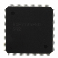
HD64F7145F50 Renesas Electronics America, HD64F7145F50 Datasheet - Page 678

HD64F7145F50
Manufacturer Part Number
HD64F7145F50
Description
IC SUPERH MCU FLASH 256K FP144F
Manufacturer
Renesas Electronics America
Series
SuperH® SH7144r
Datasheet
1.HD64F7144F50V.pdf
(932 pages)
Specifications of HD64F7145F50
Core Processor
SH-2
Core Size
32-Bit
Speed
50MHz
Connectivity
EBI/EMI, I²C, SCI
Peripherals
DMA, POR, PWM, WDT
Number Of I /o
98
Program Memory Size
256KB (256K x 8)
Program Memory Type
FLASH
Ram Size
8K x 8
Voltage - Supply (vcc/vdd)
3 V ~ 3.6 V
Data Converters
A/D 8x10b
Oscillator Type
Internal
Operating Temperature
-20°C ~ 75°C
Package / Case
144-LQFP
Lead Free Status / RoHS Status
Contains lead / RoHS non-compliant
Eeprom Size
-
Available stocks
Company
Part Number
Manufacturer
Quantity
Price
Part Number:
HD64F7145F50
Manufacturer:
RENESAS/瑞萨
Quantity:
20 000
Company:
Part Number:
HD64F7145F50V
Manufacturer:
Renesas Electronics America
Quantity:
10 000
Part Number:
HD64F7145F50V
Manufacturer:
RENESAS/瑞萨
Quantity:
20 000
- Current page: 678 of 932
- Download datasheet (6Mb)
17. Pin Function Controller (PFC)
5. When the system uses the external space, the data I/O pins must be set as follows according to
6. If a power-on reset is input to the RES pin in the state where the pin is a general output pin and
Rev.4.00 Mar. 27, 2008 Page 632 of 882
REJ09B0108-0400
the bus sizes in the CS space set by the bus control register 1 (BCR1).
⎯ When the CS space is the byte size (8-bit size), set all pins, D7 to D0, as data I/O pins.
⎯ When the CS space is the word size (16-bit size), set all pins, D15 to D0, as data I/O pins.
⎯ When the CS space is the longword size (32-bit size), set all pins, D31 to D0, as data I/O
set to output 1 (that is, the port control register is in the general I/O state, port I/O register is 1,
and port data register is 1), a low level may occur in the pin at a power-on reset input. To avoid
this low level from occurring, input a power-on reset after clearing the port I/O register to 0
(general input). The low level above will not occur when an internal power-on reset is input
due to a WDT overflow.
pins.
If the contents in the external space are read by settings other than above ways, no correct
data can be latched. This note applies to entire space, CS0 to CS7.
Related parts for HD64F7145F50
Image
Part Number
Description
Manufacturer
Datasheet
Request
R

Part Number:
Description:
KIT STARTER FOR M16C/29
Manufacturer:
Renesas Electronics America
Datasheet:

Part Number:
Description:
KIT STARTER FOR R8C/2D
Manufacturer:
Renesas Electronics America
Datasheet:

Part Number:
Description:
R0K33062P STARTER KIT
Manufacturer:
Renesas Electronics America
Datasheet:

Part Number:
Description:
KIT STARTER FOR R8C/23 E8A
Manufacturer:
Renesas Electronics America
Datasheet:

Part Number:
Description:
KIT STARTER FOR R8C/25
Manufacturer:
Renesas Electronics America
Datasheet:

Part Number:
Description:
KIT STARTER H8S2456 SHARPE DSPLY
Manufacturer:
Renesas Electronics America
Datasheet:

Part Number:
Description:
KIT STARTER FOR R8C38C
Manufacturer:
Renesas Electronics America
Datasheet:

Part Number:
Description:
KIT STARTER FOR R8C35C
Manufacturer:
Renesas Electronics America
Datasheet:

Part Number:
Description:
KIT STARTER FOR R8CL3AC+LCD APPS
Manufacturer:
Renesas Electronics America
Datasheet:

Part Number:
Description:
KIT STARTER FOR RX610
Manufacturer:
Renesas Electronics America
Datasheet:

Part Number:
Description:
KIT STARTER FOR R32C/118
Manufacturer:
Renesas Electronics America
Datasheet:

Part Number:
Description:
KIT DEV RSK-R8C/26-29
Manufacturer:
Renesas Electronics America
Datasheet:

Part Number:
Description:
KIT STARTER FOR SH7124
Manufacturer:
Renesas Electronics America
Datasheet:

Part Number:
Description:
KIT STARTER FOR H8SX/1622
Manufacturer:
Renesas Electronics America
Datasheet:


