DF2378RVFQ34V Renesas Electronics America, DF2378RVFQ34V Datasheet - Page 66
DF2378RVFQ34V
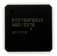
Manufacturer Part Number
DF2378RVFQ34V
Description
IC H8S MCU FLASH 512K 144LQFP
Manufacturer
Renesas Electronics America
Series
H8® H8S/2300r
Specifications of DF2378RVFQ34V
Core Processor
H8S/2000
Core Size
16-Bit
Speed
34MHz
Connectivity
I²C, IrDA, SCI, SmartCard
Peripherals
DMA, POR, PWM, WDT
Number Of I /o
97
Program Memory Size
512KB (512K x 8)
Program Memory Type
FLASH
Ram Size
32K x 8
Voltage - Supply (vcc/vdd)
3 V ~ 3.6 V
Data Converters
A/D 16x10b; D/A 6x8b
Oscillator Type
Internal
Operating Temperature
-20°C ~ 75°C
Package / Case
144-LQFP
For Use With
YLCDRSK2378 - KIT DEV EVAL H8S/2378 LCDYR0K42378FC000BA - KIT EVAL FOR H8S/2378HS0005KCU11H - EMULATOR E10A-USB H8S(X),SH2(A)EDK2378 - DEV EVAL KIT FOR H8S/2378
Lead Free Status / RoHS Status
Lead free / RoHS Compliant
Eeprom Size
-
Available stocks
Company
Part Number
Manufacturer
Quantity
Price
Company:

Part Number:
DF2378RVFQ34V
Manufacturer:
Renesas Electronics America
Quantity:
10 000


Table 21.8 (2) Useable Area for Erasure in User Program Mode................................................. 914
Table 21.8 (3) Useable Area for Programming in User Boot Mode ............................................. 916
Table 21.8 (4) Useable Area for Erasure in User Boot Mode....................................................... 918
Table 21.9
Table 21.10 Software Protection ................................................................................................. 921
Table 21.11 Inquiry and Selection Commands ........................................................................... 928
Table 21.12 Programming/Erasing Command ............................................................................ 941
Table 21.13 Status Code.............................................................................................................. 950
Table 21.14 Error Code............................................................................................................... 951
Table 21.15 User Branch Processing Start Intervals ................................................................... 952
Section 23 Clock Pulse Generator ..................................................................... 955
Table 23.1
Table 23.2
Table 23.3
Section 24 Power-Down Modes ........................................................................ 965
Table 24.1
Table 24.2
Table 24.3
Section 26 Electrical Characteristics ............................................................... 1019
Table 26.1
Table 26.2
Table 26.3
Table 26.4
Table 26.5
Table 26.6
Table 26.7
Table 26.8
Table 26.9
Table 26.10 Timing of On-Chip Peripheral Modules................................................................ 1030
Table 26.11 A/D Conversion Characteristics ............................................................................ 1032
Table 26.12 D/A Conversion Characteristics ............................................................................ 1032
Table 26.13 Flash Memory Characteristics (0.35-μm F-ZTAT Version) ................................. 1033
Table 26.14 Absolute Maximum Ratings.................................................................................. 1035
Table 26.15 DC Characteristics................................................................................................. 1036
Table 26.16 DC Characteristics................................................................................................. 1037
Table 26.17 Permissible Output Currents ................................................................................. 1038
Table 26.18 Clock Timing......................................................................................................... 1039
Table 26.19 Control Signal Timing........................................................................................... 1040
Rev.7.00 Mar. 18, 2009 page lxiv of lxvi
REJ09B0109-0700
Hardware Protection................................................................................................ 920
Damping Resistance Value ..................................................................................... 958
Crystal Resonator Characteristics............................................................................ 959
External Clock Input Conditions ............................................................................. 960
Operating Modes and Internal states of the LSI ...................................................... 966
Oscillation Stabilization Time Settings ................................................................... 975
φ Pin State in Each Processing State ....................................................................... 979
Absolute Maximum Ratings.................................................................................. 1019
DC Characteristics (1) ........................................................................................... 1020
DC Characteristics (2) ........................................................................................... 1021
Permissible Output Currents ................................................................................. 1022
Clock Timing......................................................................................................... 1024
Control Signal Timing........................................................................................... 1025
Bus Timing (1) ...................................................................................................... 1026
Bus Timing (2) ...................................................................................................... 1027
DMAC and EXDMAC Timing ............................................................................. 1029
Related parts for DF2378RVFQ34V
Image
Part Number
Description
Manufacturer
Datasheet
Request
R

Part Number:
Description:
KIT STARTER FOR M16C/29
Manufacturer:
Renesas Electronics America
Datasheet:

Part Number:
Description:
KIT STARTER FOR R8C/2D
Manufacturer:
Renesas Electronics America
Datasheet:

Part Number:
Description:
R0K33062P STARTER KIT
Manufacturer:
Renesas Electronics America
Datasheet:

Part Number:
Description:
KIT STARTER FOR R8C/23 E8A
Manufacturer:
Renesas Electronics America
Datasheet:

Part Number:
Description:
KIT STARTER FOR R8C/25
Manufacturer:
Renesas Electronics America
Datasheet:

Part Number:
Description:
KIT STARTER H8S2456 SHARPE DSPLY
Manufacturer:
Renesas Electronics America
Datasheet:

Part Number:
Description:
KIT STARTER FOR R8C38C
Manufacturer:
Renesas Electronics America
Datasheet:

Part Number:
Description:
KIT STARTER FOR R8C35C
Manufacturer:
Renesas Electronics America
Datasheet:

Part Number:
Description:
KIT STARTER FOR R8CL3AC+LCD APPS
Manufacturer:
Renesas Electronics America
Datasheet:
Part Number:
Description:
KIT STARTER FOR RX610
Manufacturer:
Renesas Electronics America
Datasheet:

Part Number:
Description:
KIT STARTER FOR R32C/118
Manufacturer:
Renesas Electronics America
Datasheet:

Part Number:
Description:
KIT DEV RSK-R8C/26-29
Manufacturer:
Renesas Electronics America
Datasheet:

Part Number:
Description:
KIT STARTER FOR SH7124
Manufacturer:
Renesas Electronics America
Datasheet:

Part Number:
Description:
KIT STARTER FOR H8SX/1622
Manufacturer:
Renesas Electronics America
Datasheet:

Part Number:
Description:
KIT DEV FOR SH7203
Manufacturer:
Renesas Electronics America
Datasheet: