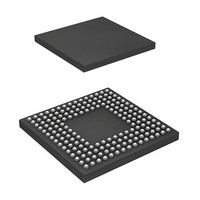
DF2552BR26DV Renesas Electronics America, DF2552BR26DV Datasheet - Page 832

DF2552BR26DV
Manufacturer Part Number
DF2552BR26DV
Description
IC H8S/2552 MCU FLASH 176-LFBGA
Manufacturer
Renesas Electronics America
Series
H8® H8S/2500r
Specifications of DF2552BR26DV
Core Processor
H8S/2000
Core Size
16-Bit
Speed
26MHz
Connectivity
I²C, SCI
Peripherals
POR, PWM, WDT
Number Of I /o
104
Program Memory Size
512KB (512K x 8)
Program Memory Type
FLASH
Ram Size
32K x 8
Voltage - Supply (vcc/vdd)
3 V ~ 5.5 V
Data Converters
A/D 16x10b; D/A 2x8b
Oscillator Type
Internal
Operating Temperature
-40°C ~ 85°C
Package / Case
176-LFBGA
Lead Free Status / RoHS Status
Lead free / RoHS Compliant
Eeprom Size
-
Available stocks
Company
Part Number
Manufacturer
Quantity
Price
Company:
Part Number:
DF2552BR26DV
Manufacturer:
Renesas Electronics America
Quantity:
10 000
- Current page: 832 of 980
- Download datasheet (6Mb)
Section 21 Clock Pulse Generator
21.3
The PLL circuit multiplies the frequency from the clock pulse generator by one or two. The
multiplication ratio is set by the STC1 and STC0 bits in LPWRCR. At the setting, the phase of the
rising edge of an internal clock is controlled to match that of the rising edge of the EXTAL pin.
When changing the multiplication ratio of the PLL circuit, the operation differs according to the
setting of the STCS bit in SCKCR.
When the STCS bit is 0, the changed multiplication ratio is valid after software standby mode or
watch mode is entered. The transition time is set by the STS2 to STS0 bits in the standby control
register (SBYCR). For details on SBYCR, see section 22.1.1, Standby Control Register (SBYCR).
1. In the initial state, the multiplication ratio of the PLL circuit is 1.
2. The transition time is set by the STS2 to STS0 bits.
3. The multiplication ratio is set by the STC1 and STC0 bits, and software standby mode or
Rev. 6.00 Sep. 24, 2009 Page 784 of 928
REJ09B0099-0600
External
clock 1
External
clock 2
Operation
Port output
External
clock
switching
circuit
EXTAL
Internal
clock φ
External
interrupt
watch mode is entered.
Clock switching
PLL Circuit
request
(1)
Figure 21.7 External Clock Switching Timing (Examples)
(1) Port output (clock switching)
(2) Transition to software standby mode
(3) External clock switchover
(4) External interrupt generation
(5) Interrupt exception handling
SLEEP instruction
Active (external clock2)
(An interrupt should be input 200 ns or more after transition to software standby mode.)
execution
(2)
200ns or more
(3)
Software standby mode
(4)
standby time
(5)
Interrupt exception handling
Active (external clock1)
Related parts for DF2552BR26DV
Image
Part Number
Description
Manufacturer
Datasheet
Request
R

Part Number:
Description:
KIT STARTER FOR M16C/29
Manufacturer:
Renesas Electronics America
Datasheet:

Part Number:
Description:
KIT STARTER FOR R8C/2D
Manufacturer:
Renesas Electronics America
Datasheet:

Part Number:
Description:
R0K33062P STARTER KIT
Manufacturer:
Renesas Electronics America
Datasheet:

Part Number:
Description:
KIT STARTER FOR R8C/23 E8A
Manufacturer:
Renesas Electronics America
Datasheet:

Part Number:
Description:
KIT STARTER FOR R8C/25
Manufacturer:
Renesas Electronics America
Datasheet:

Part Number:
Description:
KIT STARTER H8S2456 SHARPE DSPLY
Manufacturer:
Renesas Electronics America
Datasheet:

Part Number:
Description:
KIT STARTER FOR R8C38C
Manufacturer:
Renesas Electronics America
Datasheet:

Part Number:
Description:
KIT STARTER FOR R8C35C
Manufacturer:
Renesas Electronics America
Datasheet:

Part Number:
Description:
KIT STARTER FOR R8CL3AC+LCD APPS
Manufacturer:
Renesas Electronics America
Datasheet:

Part Number:
Description:
KIT STARTER FOR RX610
Manufacturer:
Renesas Electronics America
Datasheet:

Part Number:
Description:
KIT STARTER FOR R32C/118
Manufacturer:
Renesas Electronics America
Datasheet:

Part Number:
Description:
KIT DEV RSK-R8C/26-29
Manufacturer:
Renesas Electronics America
Datasheet:

Part Number:
Description:
KIT STARTER FOR SH7124
Manufacturer:
Renesas Electronics America
Datasheet:

Part Number:
Description:
KIT STARTER FOR H8SX/1622
Manufacturer:
Renesas Electronics America
Datasheet:

Part Number:
Description:
KIT DEV FOR SH7203
Manufacturer:
Renesas Electronics America
Datasheet:


