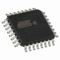
ATMEGA8-16AC Atmel, ATMEGA8-16AC Datasheet - Page 142

ATMEGA8-16AC
Manufacturer Part Number
ATMEGA8-16AC
Description
IC AVR MCU 8K 16MHZ COM 32-TQFP
Manufacturer
Atmel
Series
AVR® ATmegar
Specifications of ATMEGA8-16AC
Core Processor
AVR
Core Size
8-Bit
Speed
16MHz
Connectivity
I²C, SPI, UART/USART
Peripherals
Brown-out Detect/Reset, POR, PWM, WDT
Number Of I /o
23
Program Memory Size
8KB (4K x 16)
Program Memory Type
FLASH
Eeprom Size
512 x 8
Ram Size
1K x 8
Voltage - Supply (vcc/vdd)
4.5 V ~ 5.5 V
Data Converters
A/D 8x10b
Oscillator Type
Internal
Operating Temperature
0°C ~ 70°C
Package / Case
32-TQFP, 32-VQFP
Lead Free Status / RoHS Status
Contains lead / RoHS non-compliant
Other names
ATMEGA816AC
Available stocks
Company
Part Number
Manufacturer
Quantity
Price
- Current page: 142 of 302
- Download datasheet (6Mb)
Disabling the Receiver In contrast to the Transmitter, disabling of the Receiver will be immediate. Data from ongoing
Flushing the Receive
Buffer
Asynchronous
Data Reception
Asynchronous Clock
Recovery
142
ATmega8(L)
receptions will therefore be lost. When disabled (that is, the RXEN is set to zero) the Receiver
will no longer override the normal function of the RxD port pin. The Receiver buffer FIFO will be
flushed when the Receiver is disabled. Remaining data in the buffer will be lost
The Receiver buffer FIFO will be flushed when the Receiver is disabled (that is, the buffer will be
emptied of its contents). Unread data will be lost. If the buffer has to be flushed during normal
operation, due to for instance an error condition, read the UDR I/O location until the RXC Flag is
cleared. The following code example shows how to flush the receive buffer.
Note:
The USART includes a clock recovery and a data recovery unit for handling asynchronous data
reception. The clock recovery logic is used for synchronizing the internally generated baud rate
clock to the incoming asynchronous serial frames at the RxD pin. The data recovery logic sam-
ples and low pass filters each incoming bit, thereby improving the noise immunity of the
Receiver. The asynchronous reception operational range depends on the accuracy of the inter-
nal baud rate clock, the rate of the incoming frames, and the frame size in number of bits.
The clock recovery logic synchronizes internal clock to the incoming serial frames.
illustrates the sampling process of the start bit of an incoming frame. The sample rate is 16 times
the baud rate for Normal mode, and eight times the baud rate for Double Speed mode. The hor-
izontal arrows illustrate the synchronization variation due to the sampling process. Note the
larger time variation when using the Double Speed mode (U2X = 1) of operation. Samples
denoted zero are samples done when the RxD line is idle (that is, no communication activity).
Figure 65. Start Bit Sampling
When the clock recovery logic detects a high (idle) to low (start) transition on the RxD line, the
start bit detection sequence is initiated. Let sample 1 denote the first zero-sample as shown in
Assembly Code Example
C Code Example
(U2X = 0)
(U2X = 1)
Sample
Sample
USART_Flush:
void USART_Flush( void )
{
}
RxD
sbis UCSRA, RXC
ret
in
rjmp USART_Flush
unsigned char dummy;
while ( UCSRA & (1<<RXC) ) dummy = UDR;
1. See
r16, UDR
0
0
IDLE
“About Code Examples” on page 8
(1)
0
1
1
2
(1)
3
2
4
5
3
6
7
4
8
START
9
5
10
11
6
12
13
7
14
15
8
16
1
1
2486Z–AVR–02/11
2
BIT 0
Figure 65
3
2
Related parts for ATMEGA8-16AC
Image
Part Number
Description
Manufacturer
Datasheet
Request
R

Part Number:
Description:
IC AVR MCU 8K 16MHZ 5V 32TQFP
Manufacturer:
Atmel
Datasheet:

Part Number:
Description:
IC AVR MCU 8K 16MHZ 5V 32-QFN
Manufacturer:
Atmel
Datasheet:

Part Number:
Description:
IC AVR MCU 8K 16MHZ 5V 28DIP
Manufacturer:
Atmel
Datasheet:

Part Number:
Description:
IC AVR MCU 8K 16MHZ IND 32-TQFP
Manufacturer:
Atmel
Datasheet:

Part Number:
Description:
IC AVR MCU 8K 16MHZ COM 28-DIP
Manufacturer:
Atmel
Datasheet:

Part Number:
Description:
IC AVR MCU 8K 16MHZ IND 28-DIP
Manufacturer:
Atmel
Datasheet:

Part Number:
Description:
IC AVR MCU 8K 16MHZ COM 32-QFN
Manufacturer:
Atmel
Datasheet:

Part Number:
Description:
MCU AVR 8KB FLASH 16MHZ 32QFN
Manufacturer:
Atmel
Datasheet:

Part Number:
Description:
IC AVR MCU 8K 16MHZ IND 32-QFN
Manufacturer:
Atmel
Datasheet:

Part Number:
Description:
IC MCU AVR 8K 5V 16MHZ 32-TQFP
Manufacturer:
Atmel
Datasheet:

Part Number:
Description:
IC MCU AVR 8K 5V 16MHZ 32-QFN
Manufacturer:
Atmel
Datasheet:

Part Number:
Description:
IC MCU AVR 8K 5V 16MHZ 28-DIP
Manufacturer:
Atmel
Datasheet:

Part Number:
Description:
IC MCU AVR 8K 16MHZ 5V 32TQFP
Manufacturer:
Atmel
Datasheet:


