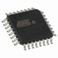
ATMEGA8-16AC Atmel, ATMEGA8-16AC Datasheet - Page 84

ATMEGA8-16AC
Manufacturer Part Number
ATMEGA8-16AC
Description
IC AVR MCU 8K 16MHZ COM 32-TQFP
Manufacturer
Atmel
Series
AVR® ATmegar
Specifications of ATMEGA8-16AC
Core Processor
AVR
Core Size
8-Bit
Speed
16MHz
Connectivity
I²C, SPI, UART/USART
Peripherals
Brown-out Detect/Reset, POR, PWM, WDT
Number Of I /o
23
Program Memory Size
8KB (4K x 16)
Program Memory Type
FLASH
Eeprom Size
512 x 8
Ram Size
1K x 8
Voltage - Supply (vcc/vdd)
4.5 V ~ 5.5 V
Data Converters
A/D 8x10b
Oscillator Type
Internal
Operating Temperature
0°C ~ 70°C
Package / Case
32-TQFP, 32-VQFP
Lead Free Status / RoHS Status
Contains lead / RoHS non-compliant
Other names
ATMEGA816AC
Available stocks
Company
Part Number
Manufacturer
Quantity
Price
- Current page: 84 of 302
- Download datasheet (6Mb)
Figure 35
shows a block diagram of the Output Compare unit. The small “n” in the register and
bit names indicates the device number (n = 1 for Timer/Counter 1), and the “x” indicates Output
Compare unit (A/B). The elements of the block diagram that are not directly a part of the Output
Compare unit are gray shaded.
Figure 35. Output Compare Unit, Block Diagram
DATA BUS
(8-bit)
TEMP (8-bit)
OCRnxH Buf. (8-bit)
OCRnxL Buf. (8-bit)
TCNTnH (8-bit)
TCNTnL (8-bit)
OCRnx Buffer (16-bit Register)
TCNTn (16-bit Counter)
OCRnxH (8-bit)
OCRnxL (8-bit)
OCRnx (16-bit Register)
=
(16-bit Comparator )
OCFnx (Int.Req.)
TOP
Waveform Generator
OCnx
BOTTOM
WGMn3:0
COMnx1:0
The OCR1x Register is double buffered when using any of the twelve Pulse Width Modulation
(PWM) modes. For the normal and Clear Timer on Compare (CTC) modes of operation, the dou-
ble buffering is disabled. The double buffering synchronizes the update of the OCR1x Compare
Register to either TOP or BOTTOM of the counting sequence. The synchronization prevents the
occurrence of odd-length, non-symmetrical PWM pulses, thereby making the output glitch-free.
The OCR1x Register access may seem complex, but this is not case. When the double buffering
is enabled, the CPU has access to the OCR1x Buffer Register, and if double buffering is dis-
abled the CPU will access the OCR1x directly. The content of the OCR1x (Buffer or Compare)
Register is only changed by a write operation (the Timer/Counter does not update this register
automatically as the TCNT1 and ICR1 Register). Therefore OCR1x is not read via the High byte
temporary register (TEMP). However, it is a good practice to read the Low byte first as when
accessing other 16-bit registers. Writing the OCR1x Registers must be done via the TEMP Reg-
ister since the compare of all 16-bit is done continuously. The High byte (OCR1xH) has to be
written first. When the High byte I/O location is written by the CPU, the TEMP Register will be
updated by the value written. Then when the Low byte (OCR1xL) is written to the lower eight
bits, the High byte will be copied into the upper 8-bits of either the OCR1x buffer or OCR1x Com-
pare Register in the same system clock cycle.
For more information of how to access the 16-bit registers refer to
“Accessing 16-bit Registers”
on page
77.
ATmega8(L)
84
2486Z–AVR–02/11
Related parts for ATMEGA8-16AC
Image
Part Number
Description
Manufacturer
Datasheet
Request
R

Part Number:
Description:
IC AVR MCU 8K 16MHZ 5V 32TQFP
Manufacturer:
Atmel
Datasheet:

Part Number:
Description:
IC AVR MCU 8K 16MHZ 5V 32-QFN
Manufacturer:
Atmel
Datasheet:

Part Number:
Description:
IC AVR MCU 8K 16MHZ 5V 28DIP
Manufacturer:
Atmel
Datasheet:

Part Number:
Description:
IC AVR MCU 8K 16MHZ IND 32-TQFP
Manufacturer:
Atmel
Datasheet:

Part Number:
Description:
IC AVR MCU 8K 16MHZ COM 28-DIP
Manufacturer:
Atmel
Datasheet:

Part Number:
Description:
IC AVR MCU 8K 16MHZ IND 28-DIP
Manufacturer:
Atmel
Datasheet:

Part Number:
Description:
IC AVR MCU 8K 16MHZ COM 32-QFN
Manufacturer:
Atmel
Datasheet:

Part Number:
Description:
MCU AVR 8KB FLASH 16MHZ 32QFN
Manufacturer:
Atmel
Datasheet:

Part Number:
Description:
IC AVR MCU 8K 16MHZ IND 32-QFN
Manufacturer:
Atmel
Datasheet:

Part Number:
Description:
IC MCU AVR 8K 5V 16MHZ 32-TQFP
Manufacturer:
Atmel
Datasheet:

Part Number:
Description:
IC MCU AVR 8K 5V 16MHZ 32-QFN
Manufacturer:
Atmel
Datasheet:

Part Number:
Description:
IC MCU AVR 8K 5V 16MHZ 28-DIP
Manufacturer:
Atmel
Datasheet:

Part Number:
Description:
IC MCU AVR 8K 16MHZ 5V 32TQFP
Manufacturer:
Atmel
Datasheet:


