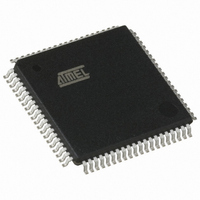
AT80C51SND1C-ROTIL Atmel, AT80C51SND1C-ROTIL Datasheet - Page 148

AT80C51SND1C-ROTIL
Manufacturer Part Number
AT80C51SND1C-ROTIL
Description
IC MCU FLASH MP3 DECODER 80-TQFP
Manufacturer
Atmel
Series
80Cr
Datasheet
1.AT80C51SND1C-ROTIL.pdf
(213 pages)
Specifications of AT80C51SND1C-ROTIL
Core Processor
8051
Core Size
8-Bit
Speed
40MHz
Connectivity
I²C, IDE/ATAPI, MMC, SPI, UART/USART, USB
Peripherals
Audio, I²S, MP3, PCM, POR, WDT
Number Of I /o
44
Program Memory Type
ROMless
Ram Size
2.25K x 8
Voltage - Supply (vcc/vdd)
2.7 V ~ 3.3 V
Data Converters
A/D 2x10b
Oscillator Type
Internal
Operating Temperature
-40°C ~ 85°C
Package / Case
80-TQFP, 80-VQFP
Lead Free Status / RoHS Status
Contains lead / RoHS non-compliant
Eeprom Size
-
Program Memory Size
-
Other names
AT80C51SND1CROTIL
Available stocks
Company
Part Number
Manufacturer
Quantity
Price
- Current page: 148 of 213
- Download datasheet (3Mb)
19.1
19.1.1
Figure 19-3. SPI Master Mode Block Diagram
Note:
19.1.2
148
Description
MSTR bit in SPCON is set to select master mode.
AT8xC51SND1C
Master Mode
Slave Mode
CLOCK
PER
MOSI/P4.1
MISO/P4.0
SCK/P4.2
SPCON.6
SS/P4.3
SPEN
The SPI controller interfaces with the C51 core through three special function registers: SPCON,
the SPI control register (see Table 133); SPSTA, the SPI status register (see Table 134); and
SPDAT, the SPI data register (see Table 135).
The SPI operates in master mode when the MSTR bit in SPCON is set.
Figure 19-3 shows the SPI block diagram in master mode. Only a master SPI module can initiate
transmissions. Software begins the transmission by writing to SPDAT. Writing to SPDAT writes
to the shift register while reading SPDAT reads an intermediate register updated at the end of
each transfer.
The Byte begins shifting out on the MOSI pin under the control of the bit rate generator. This
generator also controls the shift register of the slave peripheral through the SCK output pin. As
the Byte shifts out, another Byte shifts in from the slave peripheral on the MISO pin. The Byte is
transmitted most significant bit (MSB) first. The end of transfer is signaled by SPIF being set.
When the AT8xC51SND1C is the only master on the bus, it can be useful not to use SS pin and
get it back to I/O functionality. This is achieved by setting SSDIS bit in SPCON.
The SPI operates in slave mode when the MSTR bit in SPCON is cleared and data has been
loaded in SPDAT.
Figure 19-4 shows the SPI block diagram in slave mode. In slave mode, before a data transmis-
sion occurs, the SS pin of the slave SPI must be asserted to low level. SS must remain low until
the transmission of the Byte is complete. In the slave SPI module, data enters the shift register
through the MOSI pin under the control of the serial clock provided by the master SPI module on
the SCK input pin. When the master starts a transmission, the data in the shift register begins
shifting out on the MISO pin. The end of transfer is signaled by SPIF being set.
Bit Rate Generator
SPR2:0
SPCON.5
SPCON
SSDIS
Control and Clock Logic
SPCON.2
CPHA
SPCON.3
CPOL
I
SPSTA.4
SPSTA.6
SPSTA.7
MODF
WCOL
SPIF
8-bit Shift Register
SPDAT RD
SPDAT WR
Q
4109L–8051–02/08
Related parts for AT80C51SND1C-ROTIL
Image
Part Number
Description
Manufacturer
Datasheet
Request
R

Part Number:
Description:
DEV KIT FOR AVR/AVR32
Manufacturer:
Atmel
Datasheet:

Part Number:
Description:
INTERVAL AND WIPE/WASH WIPER CONTROL IC WITH DELAY
Manufacturer:
ATMEL Corporation
Datasheet:

Part Number:
Description:
Low-Voltage Voice-Switched IC for Hands-Free Operation
Manufacturer:
ATMEL Corporation
Datasheet:

Part Number:
Description:
MONOLITHIC INTEGRATED FEATUREPHONE CIRCUIT
Manufacturer:
ATMEL Corporation
Datasheet:

Part Number:
Description:
AM-FM Receiver IC U4255BM-M
Manufacturer:
ATMEL Corporation
Datasheet:

Part Number:
Description:
Monolithic Integrated Feature Phone Circuit
Manufacturer:
ATMEL Corporation
Datasheet:

Part Number:
Description:
Multistandard Video-IF and Quasi Parallel Sound Processing
Manufacturer:
ATMEL Corporation
Datasheet:

Part Number:
Description:
High-performance EE PLD
Manufacturer:
ATMEL Corporation
Datasheet:

Part Number:
Description:
8-bit Flash Microcontroller
Manufacturer:
ATMEL Corporation
Datasheet:

Part Number:
Description:
2-Wire Serial EEPROM
Manufacturer:
ATMEL Corporation
Datasheet:


