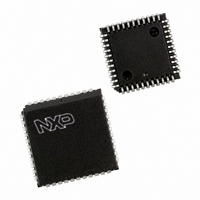
P89C662HFA/00,512 NXP Semiconductors, P89C662HFA/00,512 Datasheet - Page 80

P89C662HFA/00,512
Manufacturer Part Number
P89C662HFA/00,512
Description
IC 80C51 MCU FLASH 32K 44-PLCC
Manufacturer
NXP Semiconductors
Series
89Cr
Datasheet
1.P89C660HBA00512.pdf
(89 pages)
Specifications of P89C662HFA/00,512
Core Processor
8051
Core Size
8-Bit
Speed
33MHz
Connectivity
I²C, UART/USART
Peripherals
POR, PWM, WDT
Number Of I /o
32
Program Memory Size
32KB (32K x 8)
Program Memory Type
FLASH
Ram Size
1K x 8
Voltage - Supply (vcc/vdd)
4.75 V ~ 5.25 V
Oscillator Type
Internal
Operating Temperature
-40°C ~ 85°C
Package / Case
44-PLCC
Lead Free Status / RoHS Status
Lead free / RoHS Compliant
Eeprom Size
-
Data Converters
-
Other names
568-1270-5
935267446512
P89C662HFA
935267446512
P89C662HFA
Available stocks
Company
Part Number
Manufacturer
Quantity
Price
Company:
Part Number:
P89C662HFA/00,512
Manufacturer:
NXP Semiconductors
Quantity:
10 000
1. Parameters are valid over operating temperature range and voltage range unless otherwise specified.
2. Load capacitance for port 0, ALE, and PSEN = 100 pF, load capacitance for all other outputs = 80 pF.
3. These values are characterized but not 100% production tested.
4. At 100 kbit/s. At other bit rates this value is inversely proportional to the bit-rate of 100 kbit/s.
5. Determined by the external bus-line capacitance and the external bus-line pull-resistor, this must be < 1 s.
6. Spikes on the SDA and SCL lines with a duration of less than 3 t
7. t
Philips Semiconductors
AC ELECTRICAL CHARACTERISTICS (12 CLOCK MODE) (Continued)
T
NOTES:
2002 Oct 28
amb
I
t
t
t
t
t
t
t
t
t
t
t
t
t
t
SYMBOL
2
HD;STA
LOW
HIGH
RC
FC
SU;DAT1
SU;DAT2
SU;DAT3
HD;DAT
SU;STA
SU;STO
BUF
RD
FD
80C51 8-bit Flash microcontroller family
16KB/32KB/64KB ISP/IAP Flash with 512B/1KB/2KB/8KB RAM
C Interface
SCL = 400 pF.
I
CLCL
2
C-bus specification for bit-rates up to 100 kbit/s.
= 0 C to +70 C, V
= 1/f
OSC
START condition hold time
SCL low time
SCL high time
SCL rise time
SCL fall time
Data set-up time
SDA set-up time (before rep. START cond.)
SDA set-up time (before STOP cond.)
Data hold time
Repeated START set-up time
STOP condition set-up time
Bus free time
SDA rise time
SDA fall time
= one oscillator clock period at pin XTAL1. For 63 ns < t
CC
= 5 V
10%, or –40 C to +85 C, V
PARAMETER
CC
= 5 V
CLCL
80
5%, V
will be filtered out. Maximum capacitance on bus-lines SDA and
CLCL
SS
< 285 ns (16 MHz > f
= 0 V
14 t
14 t
14 t
INPUT
14 t
16 t
14 t
1, 2
300 ns
250 ns
250 ns
250 ns
0.3 s
P89C660/P89C662/P89C664/
1 s
1 s
0 ns
CLCL
CLCL
CLCL
CLCL
CLCL
CLCL
7
7
4
4
4
OSC
> 3.5 MHz) the I
> 20 t
> 8 t
> 4.0 s
> 4.7 s
> 4.0 s
< 0.3 s
> 4.7 s
> 4.0 s
> 4.7 s
< 0.3 s
OUTPUT
> 8 t
2
> 1 s
C interface meets the
CLCL
CLCL
–
–
P89C668
CLCL
5
5
– t
– t
4
4
4
4
6
4
4
4
6
FC
RD
Product data


