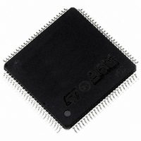
ST92F250CV2TB STMicroelectronics, ST92F250CV2TB Datasheet - Page 395

ST92F250CV2TB
Manufacturer Part Number
ST92F250CV2TB
Description
IC MCU 256K FLASH 100-TQFP
Manufacturer
STMicroelectronics
Series
ST9r
Datasheet
1.ST92F150CV1TB.pdf
(429 pages)
Specifications of ST92F250CV2TB
Core Processor
ST9
Core Size
8/16-Bit
Speed
24MHz
Connectivity
CAN, I²C, LIN, SCI, SPI
Peripherals
DMA, LVD, POR, PWM, WDT
Number Of I /o
80
Program Memory Size
256KB (256K x 8)
Program Memory Type
FLASH
Eeprom Size
1K x 8
Ram Size
8K x 8
Voltage - Supply (vcc/vdd)
4.5 V ~ 5.5 V
Data Converters
A/D 16x10b
Oscillator Type
Internal
Operating Temperature
-40°C ~ 105°C
Package / Case
100-TQFP, 100-VQFP
Processor Series
ST92F25x
Core
ST9
Data Bus Width
8 bit, 16 bit
Data Ram Size
8 KB
Interface Type
CAN, I2C, SCI, SPI
Maximum Clock Frequency
24 MHz
Number Of Programmable I/os
80
Number Of Timers
5 x 16 bit
Operating Supply Voltage
4.5 V to 5.5 V
Maximum Operating Temperature
+ 105 C
Mounting Style
SMD/SMT
Development Tools By Supplier
ST92F150-EPB
Minimum Operating Temperature
- 40 C
On-chip Adc
16 bit x 10 bit
Lead Free Status / RoHS Status
Lead free / RoHS Compliant
Other names
497-2140
Available stocks
Company
Part Number
Manufacturer
Quantity
Price
- Current page: 395 of 429
- Download datasheet (8Mb)
SPI TIMING TABLE
(V
Note:
Measurement points are V
(1) Values guaranteed by design.
Legend:
Tck = INTCLK period = Crystal Oscillator Clock period when CLOCK1 is not divided by 2;
N° Symbol
10
11
12
13
1
2
3
4
5
6
7
8
9
DD
= 5V ± 10%, T
t
t
t
SPI_H
SPI_L
t
t
f
t
t
t
Lead
t
t
Hold
Rise
Lag
SPI
SPI
Fall
SU
t
t
Dis
t
H
A
V
SPI frequency
SPI clock period
Enable lead time
Enable lag time
Clock (SCK) high time
Clock (SCK) low time
Data set-up time
Data hold time (inputs)
Access time (time to data active
from high impedance state)
Disable time (hold time to high im-
pedance state)
Data valid
Data hold time (outputs)
Rise time
(20% V
Fall time
(70% V
2 x Crystal Oscillator Clock period when CLOCK1 is divided by 2;
Crystal Oscillator Clock period x PLL factor when the PLL is enabled.
A
OL
DD
DD
=
, V
to 70% V
to 20% V
–
OH
Parameter
40°C to +125°C, C
, V
IL
and V
DD
DD
, C
, C
IH
L
L
in the SPI Timing Diagram.
ST92F124/F150/F250 - ELECTRICAL CHARACTERISTICS
= 200pF)
= 200pF)
Load
Master
Slave
Master
Slave
Slave
Slave
Master
Slave
Master
Slave
Master
Slave
Master
Slave
Slave
Master (before capture edge)
Slave (after enable edge)
Master (before capture edge)
Slave (after enable edge)
Outputs: SCK,MOSI,MISO
Inputs: SCK,MOSI,MISO,SS
Outputs: SCK,MOSI,MISO
Inputs: SCK,MOSI,MISO,SS
= 50pF, f
Condition
INTCLK
= 24MHz, unless otherwise specified)
f
INTCLK
4 x Tck
2 x Tck
Tck / 4
Tck / 4
Min
40
40
80
90
80
90
40
40
40
40
0
0
0
/ 128
Value
(1)
f
f
INTCLK
INTCLK
Max
120
240
120
100
100
100
100
/ 4
/ 2
395/429
MHz
Unit
μs
μs
ns
ns
ns
ns
ns
ns
ns
ns
ns
ns
ns
ns
ns
ns
ns
1
Related parts for ST92F250CV2TB
Image
Part Number
Description
Manufacturer
Datasheet
Request
R

Part Number:
Description:
STMicroelectronics [RIPPLE-CARRY BINARY COUNTER/DIVIDERS]
Manufacturer:
STMicroelectronics
Datasheet:

Part Number:
Description:
STMicroelectronics [LIQUID-CRYSTAL DISPLAY DRIVERS]
Manufacturer:
STMicroelectronics
Datasheet:

Part Number:
Description:
BOARD EVAL FOR MEMS SENSORS
Manufacturer:
STMicroelectronics
Datasheet:

Part Number:
Description:
NPN TRANSISTOR POWER MODULE
Manufacturer:
STMicroelectronics
Datasheet:

Part Number:
Description:
TURBOSWITCH ULTRA-FAST HIGH VOLTAGE DIODE
Manufacturer:
STMicroelectronics
Datasheet:

Part Number:
Description:
Manufacturer:
STMicroelectronics
Datasheet:

Part Number:
Description:
DIODE / SCR MODULE
Manufacturer:
STMicroelectronics
Datasheet:

Part Number:
Description:
DIODE / SCR MODULE
Manufacturer:
STMicroelectronics
Datasheet:

Part Number:
Description:
Search -----> STE16N100
Manufacturer:
STMicroelectronics
Datasheet:

Part Number:
Description:
Search ---> STE53NA50
Manufacturer:
STMicroelectronics
Datasheet:

Part Number:
Description:
NPN Transistor Power Module
Manufacturer:
STMicroelectronics
Datasheet:

Part Number:
Description:
DIODE / SCR MODULE
Manufacturer:
STMicroelectronics
Datasheet:


