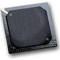
MPC564CVR40 Freescale Semiconductor, MPC564CVR40 Datasheet - Page 129

MPC564CVR40
Manufacturer Part Number
MPC564CVR40
Description
IC MPU 32BIT W/CODE COMP 388PBGA
Manufacturer
Freescale Semiconductor
Series
MPC5xxr
Specifications of MPC564CVR40
Core Processor
PowerPC
Core Size
32-Bit
Speed
40MHz
Connectivity
CAN, EBI/EMI, SCI, SPI, UART/USART
Peripherals
POR, PWM, WDT
Number Of I /o
56
Program Memory Size
512KB (512K x 8)
Program Memory Type
FLASH
Ram Size
32K x 8
Voltage - Supply (vcc/vdd)
2.5 V ~ 2.7 V
Data Converters
A/D 32x10b
Oscillator Type
External
Operating Temperature
-40°C ~ 85°C
Package / Case
388-BGA
Processor Series
MPC5xx
Core
PowerPC
Data Bus Width
32 bit
Data Ram Size
32 KB
Interface Type
CAN, JTAG, QSPI, SCI, SPI, UART
Maximum Clock Frequency
40 MHz
Number Of Programmable I/os
56
Number Of Timers
2
Maximum Operating Temperature
+ 85 C
Mounting Style
SMD/SMT
Minimum Operating Temperature
- 40 C
On-chip Adc
2 (10 bit, 32 Channel)
For Use With
MPC564EVB - KIT EVAL FOR MPC561/562/563/564
Lead Free Status / RoHS Status
Lead free / RoHS Compliant
Eeprom Size
-
Lead Free Status / Rohs Status
Details
Available stocks
Company
Part Number
Manufacturer
Quantity
Price
Company:
Part Number:
MPC564CVR40
Manufacturer:
Freescale Semiconductor
Quantity:
10 000
- Current page: 129 of 1420
- Download datasheet (11Mb)
Nexus mode is exited by:
2.6
During reset, a 130-µA (maximum) resistor “weakly pulls” all input signals, with the exception of the
power-supply and clock-related signals, to a value based on conditions described in
“Electrical
CLKOUT, HRESET, and SRESET) are pulled only by the pull-up/pull-down.
2.6.1
The reset configuration word (RCW) defines the post-reset functionality of some multiplexed signals. For
details on these signals and how they are configured, refer to Section 7.5.2, “Hard Reset Configuration
Word.”
The 2.6-V bus related signals have selectable output buffer drive strengths that are controlled by the COM0
bit in the USIU’s system clock and reset control register (SCCR). The control is as follows:
2.6.2
While HRESET is asserted, the reset-configuration value is latched from the data bus into various bits on
the part. The function of many signals depends upon the value latched. If the value on the data bus changes,
then the function of various signals may also change. This is especially true if the reset configuration word
(RCW) comes from the Flash, because the Flash does not drive the RCW until 256 clocks after the start of
Freescale Semiconductor
PORESET/TRST
JCOMP/RSTI
•
•
•
•
TMS/EVTI
Drive JCOMP/RSTI high
Hold JCOMP/RSTI low to reset Nexus port
Hold TMS/EVTI high to disable Nexus mode at least 4 clocks before driving JCOMP/RSTI high
Drive JCOMP/RSTI high
Reset State
MDI0
Characteristics.” In reset state, all I/O signals become inputs, and all outputs (except for
0 = 2.6-V bus signals full drive (50-pF load)
1 = 2.6-V bus signals reduced drive (25-pF load)
Signal Functionality Configuration Out of Reset
Signal State During Reset
Figure 2-6. Debug Mode Selection (Nexus)
MPC561/MPC563 Reference Manual, Rev. 1.2
Enable and
Configure Nexus
Nexus On
Nexus Off
Appendix F,
Signal Descriptions
T
2-31
Related parts for MPC564CVR40
Image
Part Number
Description
Manufacturer
Datasheet
Request
R

Part Number:
Description:
MPC5 1K0 5%
Manufacturer:
TE Connectivity
Datasheet:

Part Number:
Description:
MPC5 500R 5%
Manufacturer:
TE Connectivity
Datasheet:

Part Number:
Description:
MPC5 5K0 5%
Manufacturer:
Tyco Electronics
Datasheet:

Part Number:
Description:
MPC5 5R0 5%
Manufacturer:
Tyco Electronics
Datasheet:

Part Number:
Description:
MPC5 50K 5%
Manufacturer:
Tyco Electronics
Datasheet:

Part Number:
Description:
MPC5 1R0 5%
Manufacturer:
Tyco Electronics
Datasheet:
Part Number:
Description:
Manufacturer:
Freescale Semiconductor, Inc
Datasheet:
Part Number:
Description:
Manufacturer:
Freescale Semiconductor, Inc
Datasheet:
Part Number:
Description:
Manufacturer:
Freescale Semiconductor, Inc
Datasheet:
Part Number:
Description:
Manufacturer:
Freescale Semiconductor, Inc
Datasheet:
Part Number:
Description:
Manufacturer:
Freescale Semiconductor, Inc
Datasheet:


