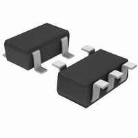
BD5242G-TR Rohm Semiconductor, BD5242G-TR Datasheet - Page 8

BD5242G-TR
Manufacturer Part Number
BD5242G-TR
Description
IC DETECTOR VOLT 4.2V ODRN 5SSOP
Manufacturer
Rohm Semiconductor
Type
Simple Reset/Power-On Resetr
Series
-r
Specifications of BD5242G-TR
Number Of Voltages Monitored
1
Output
Open Drain or Open Collector
Reset
Active Low
Voltage - Threshold
4.2V
Operating Temperature
-40°C ~ 105°C
Mounting Type
Surface Mount
Package / Case
5-SSOP
Reset Timeout
-
Lead Free Status / RoHS Status
Lead free / RoHS Compliant
Reset Timeout
-
Lead Free Status / Rohs Status
Lead free / RoHS Compliant
Available stocks
Company
Part Number
Manufacturer
Quantity
Price
Company:
Part Number:
BD5242G-TR
Manufacturer:
ROHM
Quantity:
72 000
Company:
Part Number:
BD5242G-TR
Manufacturer:
VISHAY
Quantity:
9 150
Part Number:
BD5242G-TR
Manufacturer:
ROHM/罗姆
Quantity:
20 000
Operation Notes
1 . Absolute maximum range
2 . GND potential
3 . Electrical Characteristics
4 . Bypass Capacitor for Noise Rejection
5 . Short Circuit between Terminal and Soldering
6 . Electromagnetic Field
7 .
8 .
9 .
10. This IC has extremely high impedance terminals. Small leak current due to the uncleanness of PCB surface might cause
11. External parameters
12. Power on reset operation
13. Precautions for board inspection
14. When the power supply, is turned on because of in certain cases, momentary Rash-current flow into the IC at the logic
© 2009 ROHM Co., Ltd. All rights reserved.
BD52□□G, BD52□□FVE, BD53□□G, BD53□□FVE series
www.rohm.com
Absolute Maximum Ratings are those values beyond which the life of a device may be destroyed. We cannot be defined the
failure mode, such as short mode or open mode. Therefore a physical security countermeasure, like fuse, is to be given
when a specific mode to be beyond absolute maximum ratings is considered.
GND terminal should be a lowest voltage potential every state.
Please make sure all pins, which are over ground even if, include transient feature.
Be sure to check the electrical characteristics that are one the tentative specification will be changed by temperature,
supply voltage, and external circuit.
Please put into the capacitor of 1µF or more between VDD pin and GND, and the capacitor of about 1000pF between VOUT
pin and GND, to reject noise. If extremely big capacitor is used, transient response might be late. Please confirm sufficiently
for the point.
Don’t short-circuit between Output pin and VDD pin, Output pin and GND pin, or VDD pin and GND pin. When soldering the
IC on circuit board, please be unusually cautious about the orientation and the position of the IC. When the orientation is
mistaken the IC may be destroyed.
Mal-function may happen when the device is used in the strong electromagnetic field.
unexpected operations. Application values in these conditions should be selected carefully. If the leakage is assumed
between the VOUT terminal and the GND terminal, the pull-up resistor should be less than 1/10 of the assumed leak
resistance. If 10MΩ leakage is assumed between the CT terminal and the GND terminal, 1MΩ connection between the CT
terminal and the V
connected to CT terminal, so please consider the delay time that is decided by τ×RCT×CCT changes.
The recommended parameter range for C
etc) that can affect characteristics. Please verify and confirm using practical applications.
Please note that the power on reset output varies with the VDD rise up time. Please verify the actual operation.
Connecting low-impedance capacitors to run inspections with the board may produce stress on the IC. Therefore, be
certain to use proper discharge procedure before each process of the test operation.
To prevent electrostatic accumulation and discharge in the assembly process, thoroughly ground yourself and any
equipment that could sustain ESD damage, and continue observing ESD-prevention procedures in all handing, transfer
and storage operations. Before attempting to connect components to the test setup, make certain that the power supply is
OFF. Likewise, be sure the power supply is OFF before removing any component connected to the test setup.
unsettled, the couple capacitance, GND pattern of width and leading line must be considered.
A VDD -GND capacitor (as close connection as possible) should be used in high V
The VDD line inpedance might cause oscillation because of the detection current.
Lower than the mininum input voltage makes the V
DD
terminal would be recommended. The value of R
T
is 100pF~0.1µF and RL is 50kΩ~1MΩ. There are many factors (board layout,
OUT
high impedance, and it must be V
8/9
CT
depends on the external resistor that is
DD
line impedance condition.
DD
in pull up (V
Technical Note
2009.06 - Rev.B
DD
) condition.


