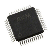
AK4358VQ AKM Semiconductor Inc, AK4358VQ Datasheet - Page 24

AK4358VQ
Manufacturer Part Number
AK4358VQ
Description
IC DAC 24BIT SERIAL 48LQFP
Manufacturer
AKM Semiconductor Inc
Datasheet
1.AK4358VQ.pdf
(36 pages)
Specifications of AK4358VQ
Number Of Bits
24
Data Interface
I²S, Serial
Number Of Converters
8
Voltage Supply Source
Analog and Digital
Operating Temperature
-40°C ~ 85°C
Mounting Type
Surface Mount
Package / Case
48-LFQFP
Lead Free Status / RoHS Status
Lead free / RoHS Compliant
Power Dissipation (max)
-
Settling Time
-
Other names
974-1008-2
Available stocks
Company
Part Number
Manufacturer
Quantity
Price
Company:
Part Number:
AK4358VQ
Manufacturer:
AKM Semiconductor Inc
Quantity:
1 951
Company:
Part Number:
AK4358VQ
Manufacturer:
AKM
Quantity:
11 050
Company:
Part Number:
AK4358VQ-L
Manufacturer:
ELPIDA
Quantity:
32
Part Number:
AK4358VQ-L
Manufacturer:
AKM
Quantity:
20 000
Company:
Part Number:
AK4358VQP-L
Manufacturer:
AKM Semiconductor Inc
Quantity:
10 000
■
The AK4358 controls its functions via registers. 2 types of control mode write internal registers. In the I
chip address is determined by the state of the CAD0 and CAD1 inputs. In 3-wire mode, the CAD1 input is fixed to “1” and
Chip Address C0 is determined by the state of the CAD0 pin. PDN = “L” initializes the registers to their default values.
Writing “0” to the RSTN bit resets the internal timing circuit, but the register data is not initialized.
(1) 3-wire Serial Control Mode (I2C = “L”)
3-wire µP interface pins, CSN, CCLK and CDTI, write internal registers. The data on this interface consists of Chip
Address (2bits, C1/0; C1 is fixed to “1” and C0=CAD0), Read/Write (1bit; fixed to “1”, Write only), Register Address
(MSB first, 5bits) and Control Data (MSB first, 8bits). The AK4358 latches the data on the rising edge of CCLK, so data
should clocked in on the falling edge. The writing of data becomes valid by the rising edge of CSN. The clock speed of
CCLK is 5MHz (max).
MS0203-E-02
Register Control Interface
* The AK4358 does not support the read command.
* When the AK4358 is in the power down mode (PDN = “L”) or the MCLK is not provided, Writing to control
register is invalid.
CCLK
CSN
CDTI
Function
Manual Setting Mode
De-emphasis
DZFE
SMUTE
Audio data format
DSD mode
Attenuator
Slow roll-off response
C1
Table 17. Function Table (O: Supported, X: Not supported)
0
C0
1
R/W
2
C1-C0:
R/W:
A4-A0:
D7-D0:
A4
3
Figure 17. Control I/F Timing
A3
4
A2
5
Chip Address (C1= “1”, C0=CAD0)
READ/WRITE (Fixed to “1”, Write only)
Register Address
Control Data
A1
6
- 24 -
Pin set-up
A0
DIF0
7
O
X
X
X
X
X
X
D7
8
D6
9
D5
10 11 12 13 14 15
D4
Register set-up
D3
O
O
O
O
O
O
O
O
D2
D1
D0
2
C-bus mode, the
[AK4358]
2009/05


