MC9S08AC32CPUE Freescale Semiconductor, MC9S08AC32CPUE Datasheet - Page 149
MC9S08AC32CPUE
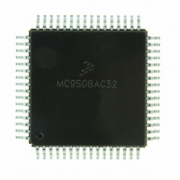
Manufacturer Part Number
MC9S08AC32CPUE
Description
IC MCU 8BIT 32K FLASH 64-LQFP
Manufacturer
Freescale Semiconductor
Series
HCS08r
Datasheet
1.MC9S08AC60CFJE.pdf
(348 pages)
Specifications of MC9S08AC32CPUE
Core Processor
HCS08
Core Size
8-Bit
Speed
40MHz
Connectivity
I²C, SCI, SPI
Peripherals
LVD, POR, PWM, WDT
Number Of I /o
54
Program Memory Size
32KB (32K x 8)
Program Memory Type
FLASH
Ram Size
2K x 8
Voltage - Supply (vcc/vdd)
2.7 V ~ 5.5 V
Data Converters
A/D 16x10b
Oscillator Type
Internal
Operating Temperature
-40°C ~ 85°C
Package / Case
64-LQFP
Processor Series
S08AC
Core
HCS08
Data Bus Width
8 bit
Data Ram Size
2 KB
Interface Type
I2C, SCI, SPI
Maximum Clock Frequency
20 MHz
Number Of Programmable I/os
54
Number Of Timers
3
Maximum Operating Temperature
+ 85 C
Mounting Style
SMD/SMT
3rd Party Development Tools
EWS08
Development Tools By Supplier
DEMO9S08AC60E, DEMOACEX, DEMOACKIT, DCF51AC256, DC9S08AC128, DC9S08AC16, DC9S08AC60, DEMO51AC256KIT
Minimum Operating Temperature
- 40 C
On-chip Adc
10 bit, 16 Channel
Lead Free Status / RoHS Status
Lead free / RoHS Compliant
Eeprom Size
-
Lead Free Status / Rohs Status
Lead free / RoHS Compliant
Available stocks
Company
Part Number
Manufacturer
Quantity
Price
Company:

Part Number:
MC9S08AC32CPUE
Manufacturer:
Freescale Semiconductor
Quantity:
10 000
Part Number:
MC9S08AC32CPUE
Manufacturer:
FREESCALEQFP
Quantity:
20 000
Company:
Part Number:
MC9S08AC32CPUER
Manufacturer:
Freescale Semiconductor
Quantity:
10 000


9.5
The ADC module is disabled during reset or when the ADCH bits are all high. The module is idle when a
conversion has completed and another conversion has not been initiated. When idle, the module is in its
lowest power state.
The ADC can perform an analog-to-digital conversion on any of the software selectable channels. The
selected channel voltage is converted by a successive approximation algorithm into an 11-bit digital result.
In 8-bit mode, the selected channel voltage is converted by a successive approximation algorithm into a
9-bit digital result.
When the conversion is completed, the result is placed in the data registers (ADCRH and ADCRL).In
10-bit mode, the result is rounded to 10 bits and placed in ADCRH and ADCRL. In 8-bit mode, the result
is rounded to 8 bits and placed in ADCRL. The conversion complete flag (COCO) is then set and an
interrupt is generated if the conversion complete interrupt has been enabled (AIEN = 1).
The ADC module has the capability of automatically comparing the result of a conversion with the
contents of its compare registers. The compare function is enabled by setting the ACFE bit and operates
in conjunction with any of the conversion modes and configurations.
9.5.1
One of four clock sources can be selected as the clock source for the ADC module. This clock source is
then divided by a configurable value to generate the input clock to the converter (ADCK). The clock is
selected from one of the following sources by means of the ADICLK bits.
Whichever clock is selected, its frequency must fall within the specified frequency range for ADCK. If the
available clocks are too slow, the ADC will not perform according to specifications. If the available clocks
Freescale Semiconductor
ADPC9
ADPC8
Field
•
•
•
•
1
0
The bus clock, which is equal to the frequency at which software is executed. This is the default
selection following reset.
The bus clock divided by 2. For higher bus clock rates, this allows a maximum divide by 16 of the
bus clock.
ALTCLK, as defined for this MCU (See module section introduction).
The asynchronous clock (ADACK) – This clock is generated from a clock source within the ADC
module. When selected as the clock source this clock remains active while the MCU is in wait or
stop3 mode and allows conversions in these modes for lower noise operation.
Functional Description
ADC Pin Control 9 — ADPC9 is used to control the pin associated with channel AD9.
0 AD9 pin I/O control enabled
1 AD9 pin I/O control disabled
ADC Pin Control 8 — ADPC8 is used to control the pin associated with channel AD8.
0 AD8 pin I/O control enabled
1 AD8 pin I/O control disabled
Clock Select and Divide Control
Table 9-10. APCTL2 Register Field Descriptions (continued)
MC9S08AC60 Series Data Sheet, Rev. 2
Description
Chapter 9 Analog-to-Digital Converter (S08ADC10V1)
149
Related parts for MC9S08AC32CPUE
Image
Part Number
Description
Manufacturer
Datasheet
Request
R

Part Number:
Description:
Manufacturer:
Freescale Semiconductor, Inc
Datasheet:
Part Number:
Description:
Manufacturer:
Freescale Semiconductor, Inc
Datasheet:
Part Number:
Description:
Manufacturer:
Freescale Semiconductor, Inc
Datasheet:
Part Number:
Description:
Manufacturer:
Freescale Semiconductor, Inc
Datasheet:
Part Number:
Description:
Manufacturer:
Freescale Semiconductor, Inc
Datasheet:
Part Number:
Description:
Manufacturer:
Freescale Semiconductor, Inc
Datasheet:
Part Number:
Description:
Manufacturer:
Freescale Semiconductor, Inc
Datasheet:
Part Number:
Description:
Manufacturer:
Freescale Semiconductor, Inc
Datasheet:
Part Number:
Description:
Manufacturer:
Freescale Semiconductor, Inc
Datasheet:
Part Number:
Description:
Manufacturer:
Freescale Semiconductor, Inc
Datasheet:
Part Number:
Description:
Manufacturer:
Freescale Semiconductor, Inc
Datasheet:
Part Number:
Description:
Manufacturer:
Freescale Semiconductor, Inc
Datasheet:
Part Number:
Description:
Manufacturer:
Freescale Semiconductor, Inc
Datasheet:
Part Number:
Description:
Manufacturer:
Freescale Semiconductor, Inc
Datasheet:
Part Number:
Description:
Manufacturer:
Freescale Semiconductor, Inc
Datasheet: