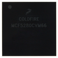
MCF5280CVM66 Freescale Semiconductor, MCF5280CVM66 Datasheet - Page 639

MCF5280CVM66
Manufacturer Part Number
MCF5280CVM66
Description
IC MPU 32BIT COLDF 256-MAPBGA
Manufacturer
Freescale Semiconductor
Series
MCF528xr
Datasheet
1.MCF5216CVM66J.pdf
(766 pages)
Specifications of MCF5280CVM66
Core Processor
Coldfire V2
Core Size
32-Bit
Speed
66MHz
Connectivity
CAN, EBI/EMI, Ethernet, I²C, SPI, UART/USART
Peripherals
DMA, LVD, POR, PWM, WDT
Number Of I /o
142
Program Memory Type
ROMless
Ram Size
64K x 8
Voltage - Supply (vcc/vdd)
2.7 V ~ 3.6 V
Data Converters
A/D 8x10b
Oscillator Type
External
Operating Temperature
-40°C ~ 85°C
Package / Case
256-MAPBGA
Controller Family/series
ColdFire
No. Of I/o's
150
Program Memory Size
2KB
Ram Memory Size
64KB
Cpu Speed
66.67MHz
Embedded Interface Type
CAN, I2C, SPI, UART
No. Of Pwm Channels
8
Rohs Compliant
Yes
Lead Free Status / RoHS Status
Lead free / RoHS Compliant
Eeprom Size
-
Program Memory Size
-
Available stocks
Company
Part Number
Manufacturer
Quantity
Price
Company:
Part Number:
MCF5280CVM66
Manufacturer:
FREESCAL
Quantity:
151
Company:
Part Number:
MCF5280CVM66
Manufacturer:
Freescale Semiconductor
Quantity:
10 000
Company:
Part Number:
MCF5280CVM66J
Manufacturer:
Freescale Semiconductor
Quantity:
10 000
Company:
Part Number:
MCF5280CVM66L
Manufacturer:
FREESCAL
Quantity:
151
- Current page: 639 of 766
- Download datasheet (9Mb)
Table 30-18
30.5.3.1.1
Some commands require extension words for addresses and/or immediate data. Addresses require two
extension words because only absolute long addressing is permitted. Longword accesses are forcibly
longword-aligned and word accesses are forcibly word-aligned. Immediate data can be 1 or 2 words long.
Byte and word data each requires a single extension word and longword data requires two extension words.
Operands and addresses are transferred most-significant word first. In the following descriptions of the
BDM command set, the optional set of extension words is defined as address, data, or operand data.
30.5.3.2 Command Sequence Diagrams
The command sequence diagram in
represents a 17-bit bus transfer. The top half of each bubble indicates the data the development system
sends to the debug module; the bottom half indicates the debug module’s response to the previous
development system commands. Command and result transactions overlap to minimize latency.
Freescale Semiconductor
15–10 Operation Specifies the command. These values are listed in
7–6
5–4
2–0
15
Bit
9
8
3
Register
Op Size
describes BDM fields.
Name
Extension Words as Required
R/W
A/D
00
0
Operation
Reserved, should be cleared.
Direction of operand transfer.
0 Data is written to the CPU or to memory from the development system.
1 The transfer is from the CPU to the development system.
Operand data size for sized operations. Addresses are expressed as 32-bit absolute values. Note
that a command performing a byte-sized memory read leaves the upper 8 bits of the response
data undefined. Referenced data is returned in the lower 8 bits of the response.
00 Byte
01 Word
10 Longword
11 Reserved
Reserved, should be cleared.
Address/data. Determines whether the register field specifies a data or address register.
0 Indicates a data register.
1 Indicates an address register.
Contains the register number in commands that operate on processor registers.
Operand Size
MCF5282 and MCF5216 ColdFire Microcontroller User’s Manual, Rev. 3
Figure 30-15. BDM Command Format
Table 30-18. BDM Field Descriptions
10
Figure 30-16
Bit Values
8 bits
16 bits
32 bits
—
0
9
Extension Word(s)
R/W
8
shows serial bus traffic for commands. Each bubble
7
Op Size
Description
6
Table
0
5
30-17.
0
4
A/D
3
2
Register
Debug Support
0
30-21
Related parts for MCF5280CVM66
Image
Part Number
Description
Manufacturer
Datasheet
Request
R
Part Number:
Description:
Manufacturer:
Freescale Semiconductor, Inc
Datasheet:
Part Number:
Description:
Manufacturer:
Freescale Semiconductor, Inc
Datasheet:
Part Number:
Description:
Manufacturer:
Freescale Semiconductor, Inc
Datasheet:
Part Number:
Description:
Manufacturer:
Freescale Semiconductor, Inc
Datasheet:
Part Number:
Description:
Manufacturer:
Freescale Semiconductor, Inc
Datasheet:
Part Number:
Description:
Manufacturer:
Freescale Semiconductor, Inc
Datasheet:
Part Number:
Description:
Manufacturer:
Freescale Semiconductor, Inc
Datasheet:
Part Number:
Description:
Manufacturer:
Freescale Semiconductor, Inc
Datasheet:
Part Number:
Description:
Manufacturer:
Freescale Semiconductor, Inc
Datasheet:
Part Number:
Description:
Manufacturer:
Freescale Semiconductor, Inc
Datasheet:
Part Number:
Description:
Manufacturer:
Freescale Semiconductor, Inc
Datasheet:
Part Number:
Description:
Manufacturer:
Freescale Semiconductor, Inc
Datasheet:
Part Number:
Description:
Manufacturer:
Freescale Semiconductor, Inc
Datasheet:
Part Number:
Description:
Manufacturer:
Freescale Semiconductor, Inc
Datasheet:
Part Number:
Description:
Manufacturer:
Freescale Semiconductor, Inc
Datasheet:


