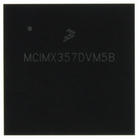
MCIMX357DVM5B Freescale Semiconductor, MCIMX357DVM5B Datasheet - Page 13

MCIMX357DVM5B
Manufacturer Part Number
MCIMX357DVM5B
Description
PROCESSOR MULTIMEDIA 400PBGA
Manufacturer
Freescale Semiconductor
Series
i.MX35r
Datasheet
1.MCIMX35WPDKJ.pdf
(148 pages)
Specifications of MCIMX357DVM5B
Core Processor
ARM11
Core Size
32-Bit
Speed
532MHz
Connectivity
1-Wire, CAN, EBI/EMI, Ethernet, I²C, MMC, SPI, SSI, UART/USART, USB OTG
Peripherals
DMA, I²S, LCD, POR, PWM, WDT
Number Of I /o
96
Program Memory Type
ROMless
Ram Size
128K x 8
Voltage - Supply (vcc/vdd)
1.33 V ~ 1.47 V
Oscillator Type
External
Operating Temperature
-20°C ~ 70°C
Package / Case
400-BGA
Operating Temperature (min)
-20C
Operating Temperature (max)
70C
Operating Temperature Classification
Commercial
Mounting
Surface Mount
Embedded Interface Type
CAN, I2C, SPI, UART, USB
Digital Ic Case Style
BGA
No. Of Pins
400
Operating Temperature Range
-20°C To +70°C
Processor Type
I.MX35
Lead Free Status / RoHS Status
Lead free / RoHS Compliant
Eeprom Size
-
Program Memory Size
-
Data Converters
-
Lead Free Status / Rohs Status
Compliant
Available stocks
Company
Part Number
Manufacturer
Quantity
Price
Company:
Part Number:
MCIMX357DVM5B
Manufacturer:
Freescale Semiconductor
Quantity:
10 000
Part Number:
MCIMX357DVM5B
Manufacturer:
FREESCALE
Quantity:
20 000
Company:
Part Number:
MCIMX357DVM5BR2
Manufacturer:
Freescale Semiconductor
Quantity:
10 000
1
2
3
4.1.1
Table 8
associated supply rail of an input or output.
Freescale Semiconductor
Core Operating Voltage
0 < f
Core Operating Voltage
0 < f
State Retention Voltage
EMI
WTDG, Timer, CCM, CSPI1
NANDF
ATA, USB generic
eSDHC1
CSI, SDIO2
JTAG
LCDC, TTM, I2C1
Supply voltage (core)
Supply voltage (I/O)
Input voltage range
Storage temperature
ESD damage immunity:
VDD is also known as QVCC.
HBM ESD classification level according to the AEC-Q100-002 standard
Corner pins max. 750 V
1
ARM
ARM
< 400 MHz
< 532 MHz
provides the recommended operating ranges. The term NVCC in this section refers to the
i.MX35 Operating Ranges
Stresses beyond those listed in
device. These are stress ratings only. Functional operation of the device at
these or any other conditions beyond those indicated in
implied. Exposure to absolute-maximum-rated conditions for extended
periods may affect device reliability.
i.MX35 Applications Processors for Industrial and Consumer Products, Rev. 9
Parameter
Parameter
Charge Device Model (CDM)
Human Body Model (HBM)
Table 7. Absolute Maximum Ratings
Table 8. i.MX35 Operating Ranges
Table 7
CAUTION
V
NVCC_EMI1,2,3
NVCC_NANDF
NVCC_ATA
NVCC_SDIO
NVCC_CSI
NVCC_JTAG
NVCC_LCDC
NVCC_CRM
may cause permanent damage to the
DD
Symbol
NVCC
VDD
Symbol
T
V
storage
V
Imax
esd
max
max
1
Table 8
Min.
1.22
1.33
1.75
1.75
1.75
1.75
1.75
1.75
1.75
1.7
1
Min.
–0.5
–0.5
–0.5
–40
—
—
is not
Typical
—
—
—
—
—
—
—
—
—
—
—
2000
Max.
500
1.47
125
3.6
3.6
Max.
1.47
1.47
3
3.6
3.6
3.6
3.6
3.6
3.6
3.6
3.6
2
—
Units
Units
o
V
V
V
V
V
V
V
V
V
V
V
V
V
V
V
C
13


