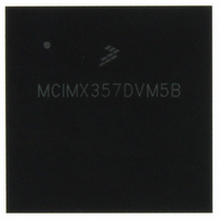
MCIMX357DVM5B Freescale Semiconductor, MCIMX357DVM5B Datasheet - Page 99

MCIMX357DVM5B
Manufacturer Part Number
MCIMX357DVM5B
Description
PROCESSOR MULTIMEDIA 400PBGA
Manufacturer
Freescale Semiconductor
Series
i.MX35r
Datasheet
1.MCIMX35WPDKJ.pdf
(148 pages)
Specifications of MCIMX357DVM5B
Core Processor
ARM11
Core Size
32-Bit
Speed
532MHz
Connectivity
1-Wire, CAN, EBI/EMI, Ethernet, I²C, MMC, SPI, SSI, UART/USART, USB OTG
Peripherals
DMA, I²S, LCD, POR, PWM, WDT
Number Of I /o
96
Program Memory Type
ROMless
Ram Size
128K x 8
Voltage - Supply (vcc/vdd)
1.33 V ~ 1.47 V
Oscillator Type
External
Operating Temperature
-20°C ~ 70°C
Package / Case
400-BGA
Operating Temperature (min)
-20C
Operating Temperature (max)
70C
Operating Temperature Classification
Commercial
Mounting
Surface Mount
Embedded Interface Type
CAN, I2C, SPI, UART, USB
Digital Ic Case Style
BGA
No. Of Pins
400
Operating Temperature Range
-20°C To +70°C
Processor Type
I.MX35
Lead Free Status / RoHS Status
Lead free / RoHS Compliant
Eeprom Size
-
Program Memory Size
-
Data Converters
-
Lead Free Status / Rohs Status
Compliant
Available stocks
Company
Part Number
Manufacturer
Quantity
Price
Company:
Part Number:
MCIMX357DVM5B
Manufacturer:
Freescale Semiconductor
Quantity:
10 000
Part Number:
MCIMX357DVM5B
Manufacturer:
FREESCALE
Quantity:
20 000
Company:
Part Number:
MCIMX357DVM5BR2
Manufacturer:
Freescale Semiconductor
Quantity:
10 000
Figure 72
Figure 73
the timing parameters.
Freescale Semiconductor
OW5
OW6
OW7
OW8
OW9
ID
ID
depicts write 0 sequence timing, and
shows write 1 sequence timing, and
Write 0 low time
Transmission time slot
Write 1/read low time
Transmission time slot
Release time
(BATT_LINE)
1-Wire bus
1-Wire bus
(BATT_LINE)
1-Wire bus
(BATT_LINE)
i.MX35 Applications Processors for Industrial and Consumer Products, Rev. 9
Parameter
Parameter
Figure 72. Write 0 Sequence Timing Diagram
Figure 73. Write 1 Sequence Timing Diagram
Table 62. WR0 Sequence Timing Parameters
Figure 74. Read Sequence Timing Diagram
Table 63. WR1/RD Timing Parameters
OW7
OW7
OW9
Figure 74
Table 62
OW5
t
Symbol
WR0_low
t
Symbol
RELEASE
t
SLOT
t
t
LOW1
SLOT
lists the timing parameters.
depicts the read sequence timing.
OW8
OW8
OW6
OW5
Min.
Min.
60
60
15
1
Typ.
Typ.
100
117
117
—
5
Max.
Max.
120
120
120
15
45
Table 63
Units
Units
µs
µs
µs
µs
µs
lists
99


