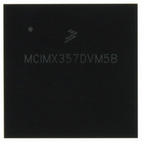
MCIMX357DVM5B Freescale Semiconductor, MCIMX357DVM5B Datasheet - Page 24

MCIMX357DVM5B
Manufacturer Part Number
MCIMX357DVM5B
Description
PROCESSOR MULTIMEDIA 400PBGA
Manufacturer
Freescale Semiconductor
Series
i.MX35r
Datasheet
1.MCIMX35WPDKJ.pdf
(148 pages)
Specifications of MCIMX357DVM5B
Core Processor
ARM11
Core Size
32-Bit
Speed
532MHz
Connectivity
1-Wire, CAN, EBI/EMI, Ethernet, I²C, MMC, SPI, SSI, UART/USART, USB OTG
Peripherals
DMA, I²S, LCD, POR, PWM, WDT
Number Of I /o
96
Program Memory Type
ROMless
Ram Size
128K x 8
Voltage - Supply (vcc/vdd)
1.33 V ~ 1.47 V
Oscillator Type
External
Operating Temperature
-20°C ~ 70°C
Package / Case
400-BGA
Operating Temperature (min)
-20C
Operating Temperature (max)
70C
Operating Temperature Classification
Commercial
Mounting
Surface Mount
Embedded Interface Type
CAN, I2C, SPI, UART, USB
Digital Ic Case Style
BGA
No. Of Pins
400
Operating Temperature Range
-20°C To +70°C
Processor Type
I.MX35
Lead Free Status / RoHS Status
Lead free / RoHS Compliant
Eeprom Size
-
Program Memory Size
-
Data Converters
-
Lead Free Status / Rohs Status
Compliant
Available stocks
Company
Part Number
Manufacturer
Quantity
Price
Company:
Part Number:
MCIMX357DVM5B
Manufacturer:
Freescale Semiconductor
Quantity:
10 000
Part Number:
MCIMX357DVM5B
Manufacturer:
FREESCALE
Quantity:
20 000
Company:
Part Number:
MCIMX357DVM5BR2
Manufacturer:
Freescale Semiconductor
Quantity:
10 000
Figure 6
4.8.1
AC electrical characteristics in
pull-down driver.
The dI/dt parameters are measured with the following methodology:
24
Duty cycle
Output pin slew rate (max. drive)
Output pin slew rate (high drive)
Output pin slew rate (standard
drive)
Output pin di/dt (max. drive)
Output pin di/dt (high drive)
Output pin di/dt (standard
drive)
Duty cycle
Output pin slew rate (max. drive)
•
•
The zero voltage source is connected between pin and load capacitance.
The current (through this source) derivative is calculated during output transitions.
shows the output pin transition time waveform.
Parameter
AC Electrical Test Parameter Definitions
Parameter
Output (at pin)
Table 15. AC Electrical Characteristics of GPIO Pins in Slow Slew Rate Mode
Table 16. AC Electrical Characteristics of GPIO Pins in Slow Slew Rate Mode
i.MX35 Applications Processors for Industrial and Consumer Products, Rev. 9
Figure 6. Output Pin Transition Time Waveform
Symbol
Table 15
Fduty
tps
tps
tps
tdit
tdit
tdit
Symbol
Fduty
tps
PA1
20%
through
[NVCC = 1.65 V–1.95 V]
Condition
[NVCC = 3.0 V–3.6 V]
80%
25 pF
25 pF
Test Condition
50 pF
25 pF
50 pF
25 pF
50 pF
50 pF
25 pF
50 pF
25 pF
50 pF
Test
—
25 pF
50 pF
Table 20
—
0.79/1.12
0.49/0.73
0.48/0.72
0.27/0.42
0.25/0.40
0.14/0.21
Rise/Fall
Min.
are not applicable for the output open drain
40
15
16
8
9
4
4
0.30/0.42
0.20/0.29
Rise/Fall
Min.
40
Typ. Rise/Fall
1.30/1.77
0.84/1.23
0.76/1.10
0.41/0.62
0.40/0.59
0.21/0.32
0.54/0.73
0.35/0.50
PA1
36
38
20
21
10
10
—
Typ.
—
80%
20%
Freescale Semiconductor
0.91/1.20
0.60/0.80
2.02/2.58
1.19/1.58
1.17/1.56
0.63/0.86
0.60/0.83
0.32/0.44
Rise/Fall
Rise/Fall
NVCC
0V
Max.
Max.
60
60
76
80
45
47
22
23
mA/ns
mA/ns
mA/ns
Units
Units
V/ns
V/ns
V/ns
V/ns
%
%


