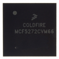
MCF5272CVM66 Freescale Semiconductor, MCF5272CVM66 Datasheet - Page 478

MCF5272CVM66
Manufacturer Part Number
MCF5272CVM66
Description
IC MPU 66MHZ COLDFIRE 196-MAPBGA
Manufacturer
Freescale Semiconductor
Series
MCF527xr
Specifications of MCF5272CVM66
Core Processor
Coldfire V2
Core Size
32-Bit
Speed
66MHz
Connectivity
EBI/EMI, Ethernet, I²C, SPI, UART/USART, USB
Peripherals
DMA, WDT
Number Of I /o
32
Program Memory Size
16KB (4K x 32)
Program Memory Type
ROM
Ram Size
1K x 32
Voltage - Supply (vcc/vdd)
3 V ~ 3.6 V
Oscillator Type
External
Operating Temperature
-40°C ~ 85°C
Package / Case
196-MAPBGA
Cpu Speed
66MHz
Embedded Interface Type
UART, QSPI, USB, TDM
Digital Ic Case Style
BGA
No. Of Pins
196
Supply Voltage Range
3V To 3.6V
Rohs Compliant
Yes
Family Name
MCF5xxx
Device Core
ColdFire
Device Core Size
32b
Frequency (max)
66MHz
Instruction Set Architecture
RISC
Supply Voltage 1 (typ)
3.3V
Operating Temp Range
-40C to 85C
Operating Temperature Classification
Industrial
Mounting
Surface Mount
Pin Count
196
Package Type
MA-BGA
Lead Free Status / RoHS Status
Lead free / RoHS Compliant
Eeprom Size
-
Data Converters
-
Lead Free Status / Rohs Status
Compliant
Available stocks
Company
Part Number
Manufacturer
Quantity
Price
Company:
Part Number:
MCF5272CVM66
Manufacturer:
MOT
Quantity:
3
Company:
Part Number:
MCF5272CVM66
Manufacturer:
Freescale Semiconductor
Quantity:
10 000
Part Number:
MCF5272CVM66
Manufacturer:
FREESCALE
Quantity:
20 000
Company:
Part Number:
MCF5272CVM66J
Manufacturer:
NSC
Quantity:
36
Company:
Part Number:
MCF5272CVM66J
Manufacturer:
Freescale Semiconductor
Quantity:
10 000
- Current page: 478 of 544
- Download datasheet (7Mb)
IEEE 1149.1 Test Access Port (JTAG)
21.4
The boundary scan register contains bits for all device signal and clock pins and associated control signals.
Bidirectional pins include a single scan bit for data (IO.Cell) as shown in
controlled by an enable cell, shown in
bidirectional pin is an input or an output. One or more bidirectional data bits can be serially connected to
a control bit as shown in
interpreted only after examining the I/O control bit to determine pin direction.
Open-drain bidirectional bits require separate input and output cells as no direction control is available
from which to determine signal direction. Programmable open-drain signals also have an enable cell
(XXX.de) to select whether the pin is open drain or push-pull. Signals with pull-up or pull-down resistors
have an associated enable cell (XXX.pu); one enable cell can control multiple resistors.
Figure 21-3
21-4
Data from
Boundary Scan Register
system
to
logic
Figure 21-8
1 = EXTEST, CLAMP, HI-Z
0 = Otherwise
MCF5272 ColdFire
Figure
show the four MCF5272 cell types.
G1
1
1
MUX
21-7. Note that when bidirectional data bits are sampled, bit data can be
Figure 21-3. Output Cell (O.Cell) (BC–1)
®
Figure
Integrated Microprocessor User’s Manual, Rev. 3
From last
Shift DR
cell
21-5. The control bit value determines whether the
G1
1
1
MUX
Clock DR
1 D
C1
Update DR
To next
cell
Figure
1 D
C1
21-6. These bits are
Freescale Semiconductor
To output
buffer
Related parts for MCF5272CVM66
Image
Part Number
Description
Manufacturer
Datasheet
Request
R
Part Number:
Description:
Mcf5272 Coldfire Integrated Microprocessor User
Manufacturer:
Freescale Semiconductor, Inc
Datasheet:

Part Number:
Description:
MCF5272 Interrupt Service Routine for the Physical Layer Interface Controller
Manufacturer:
Freescale Semiconductor / Motorola
Datasheet:
Part Number:
Description:
Manufacturer:
Freescale Semiconductor, Inc
Datasheet:
Part Number:
Description:
Manufacturer:
Freescale Semiconductor, Inc
Datasheet:
Part Number:
Description:
Manufacturer:
Freescale Semiconductor, Inc
Datasheet:
Part Number:
Description:
Manufacturer:
Freescale Semiconductor, Inc
Datasheet:
Part Number:
Description:
Manufacturer:
Freescale Semiconductor, Inc
Datasheet:
Part Number:
Description:
Manufacturer:
Freescale Semiconductor, Inc
Datasheet:
Part Number:
Description:
Manufacturer:
Freescale Semiconductor, Inc
Datasheet:
Part Number:
Description:
Manufacturer:
Freescale Semiconductor, Inc
Datasheet:
Part Number:
Description:
Manufacturer:
Freescale Semiconductor, Inc
Datasheet:
Part Number:
Description:
Manufacturer:
Freescale Semiconductor, Inc
Datasheet:
Part Number:
Description:
Manufacturer:
Freescale Semiconductor, Inc
Datasheet:
Part Number:
Description:
Manufacturer:
Freescale Semiconductor, Inc
Datasheet:
Part Number:
Description:
Manufacturer:
Freescale Semiconductor, Inc
Datasheet:


