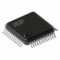
SC16C752BIB48,151 NXP Semiconductors, SC16C752BIB48,151 Datasheet - Page 6

SC16C752BIB48,151
Manufacturer Part Number
SC16C752BIB48,151
Description
IC DUAL UART 64BYTE 48LQFP
Manufacturer
NXP Semiconductors
Datasheet
1.SC16C752BIBS128.pdf
(47 pages)
Specifications of SC16C752BIB48,151
Number Of Channels
2, DUART
Package / Case
48-LFQFP
Fifo's
64 Byte
Voltage - Supply
2.5V, 3.3V, 5V
With Auto Flow Control
Yes
With False Start Bit Detection
Yes
With Modem Control
Yes
Mounting Type
Surface Mount
Voltage
2.25 V ~ 5.5 V
Data Rate
5 Mbps
Supply Voltage (max)
5.5 V
Supply Voltage (min)
2.25 V
Supply Current
4.5 mA
Maximum Operating Temperature
+ 85 C
Minimum Operating Temperature
- 40 C
Mounting Style
SMD/SMT
Operating Supply Voltage
2.5 V or 3.3 V or 5 V
Lead Free Status / RoHS Status
Lead free / RoHS Compliant
Features
-
Lead Free Status / Rohs Status
Lead free / RoHS Compliant
Other names
935274411151
SC16C752BIB48-S
SC16C752BIB48-S
SC16C752BIB48-S
SC16C752BIB48-S
Available stocks
Company
Part Number
Manufacturer
Quantity
Price
Company:
Part Number:
SC16C752BIB48,151
Manufacturer:
NXP Semiconductors
Quantity:
10 000
NXP Semiconductors
Table 2.
SC16C752B
Product data sheet
Symbol
IOW
n.c.
OPA
OPB
RESET
RIA
RIB
RTSA
RTSB
RXA
RXB
RXRDYA
RXRDYB
TXA
TXB
TXRDYA
TXRDYB
V
XTAL1
XTAL2
CC
Pin description
Pin
LQFP48 HVQFN32
15
12, 24,
25, 37
32
9
36
41
21
33
22
5
4
31
18
7
8
43
6
42
13
14
12
-
22
7
24
-
-
23
15
4
3
-
-
5
6
-
-
26
10
11
…continued
Type
I
-
O
O
I
I
I
O
O
I
I
O
O
O
O
O
O
I
I
O
All information provided in this document is subject to legal disclaimers.
Description
Input/Output Write strobe (active LOW). A LOW-to-HIGH transition on IOW
will transfer the contents of the data bus (D0 to D7) from the external CPU to an
internal register that is defined by address bits A0 to A2 and CSA and CSB.
not connected
User defined outputs. This function is associated with individual channels A
and B. The state of these pins is defined by the user through the software
settings of MCR[3]. INTA-INTB are set to active mode and OPA-OPB to a logic 0
when MCR[3] is set to a logic 1. INTA-INTB are set to the 3-state mode and
OPA-OPB to a logic 1 when MCR[3] is set to a logic 0. The output of these two
pins is HIGH after reset.
Reset. This pin will reset the internal registers and all the outputs. The UART
transmitter output and the receiver input will be disabled during reset time.
RESET is an active HIGH input.
Ring Indicator (active LOW). These inputs are associated with individual
UART channels, A and B. A logic 0 on these pins indicates the modem has
received a ringing signal from the telephone line. A LOW-to-HIGH transition on
these input pins generates a modem status interrupt, if enabled. The state of
these inputs is reflected in the Modem Status Register (MSR).
Request to Send (active LOW). These outputs are associated with individual
UART channels, A and B. A logic 0 on the RTSn pin indicates the transmitter
has data ready and waiting to send. Writing a logic 1 in the modem control
register MCR[1] will set this pin to a logic 0, indicating data is available. After a
reset these pins are set to a logic 1. These pins only affect the transmit and
receive operations when auto-RTS function is enabled via the Enhanced
Feature Register (EFR[6]) for hardware flow control operation.
Receive data input. These inputs are associated with individual serial channel
data to the SC16C752B. During the local Loopback mode, these RXn input pins
are disabled and transmit data is connected to the UART receive input internally.
Receive Ready (active LOW). RXRDYA or RXRDYB goes LOW when the
trigger level has been reached or the FIFO has at least one character. It goes
HIGH when the receive FIFO is empty.
Transmit data A, B. These outputs are associated with individual serial transmit
channel data from the SC16C752B. During the local Loopback mode, the TXn
output pin is disabled and transmit data is internally connected to the UART
receive input.
Transmit Ready (active LOW). TXRDYA or TXRDYB go LOW when there are
at least a trigger level number of spaces available or when the FIFO is empty. It
goes HIGH when the FIFO is full or not empty.
Power supply input
Crystal or external clock input. Functions as a crystal input or as an external
clock input. A crystal can be connected between XTAL1 and XTAL2 to form an
internal oscillator circuit (see
connected to this pin to provide custom data rates.
Output of the crystal oscillator or buffered clock. (See also XTAL1.) XTAL2
is used as a crystal oscillator output or a buffered clock output.
5 V, 2.2 V and 2.5 V dual UART, 5 Mbit/s (max.), with 64-byte FIFOs
Rev. 6 — 30 November 2010
Figure
13). Alternatively, an external clock can be
SC16C752B
© NXP B.V. 2010. All rights reserved.
6 of 47


