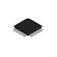
XR16L2750IM-F Exar Corporation, XR16L2750IM-F Datasheet - Page 29

XR16L2750IM-F
Manufacturer Part Number
XR16L2750IM-F
Description
IC UART FIFO 64B DUAL 48TQFP
Manufacturer
Exar Corporation
Type
IrDA or RS- 485r
Datasheet
1.XR16L2750CM-F.pdf
(48 pages)
Specifications of XR16L2750IM-F
Number Of Channels
2, DUART
Package / Case
48-TQFP
Features
*
Fifo's
64 Byte
Protocol
RS232, RS485
Voltage - Supply
2.25 V ~ 5.5 V
With Auto Flow Control
Yes
With Irda Encoder/decoder
Yes
With False Start Bit Detection
Yes
With Modem Control
Yes
With Cmos
Yes
Mounting Type
Surface Mount
Data Rate
6.25 Mbps
Supply Voltage (max)
5.5 V
Supply Voltage (min)
2.25 V
Supply Current
5 mA
Maximum Operating Temperature
+ 85 C
Minimum Operating Temperature
- 40 C
Mounting Style
SMD/SMT
Operating Supply Voltage
2.5 V or 3.3 V or 5 V
No. Of Channels
2
Uart Features
Tx/Rx FIFO Counters
Supply Voltage Range
2.25V To 5.5V
Operating Temperature Range
-40°C To +85°C
Digital Ic Case Style
TQFP
Rohs Compliant
Yes
Lead Free Status / RoHS Status
Lead free / RoHS Compliant
Lead Free Status / RoHS Status
Lead free / RoHS Compliant, Lead free / RoHS Compliant
Other names
1016-1280
Available stocks
Company
Part Number
Manufacturer
Quantity
Price
Company:
Part Number:
XR16L2750IM-F
Manufacturer:
Exar Corporation
Quantity:
10 000
Part Number:
XR16L2750IM-F
Manufacturer:
EXAR/艾科嘉
Quantity:
20 000
xr
REV. 1.2.1
MCR[1]: RTS# Output
The RTS# pin is a modem control output and may be used for automatic hardware flow control by enabled by
EFR bit-6. If the modem interface is not used, this output may be used as a general purpose output.
•
•
MCR[2]: Reserved
OP1# is not available as an output pin on the 2750. But it is available for use during Internal Loopback Mode.
In the Loopback Mode, this bit is used to write the state of the modem RI# interface signal.
MCR[3]: OP2# Output / INT Output Enable
This bit enables or disables the operation of INT, interrupt output. If INT output is not used, OP2# can be used
as a general purpose output.
•
•
MCR[4]: Internal Loopback Enable
•
•
MCR[5]: Xon-Any Enable
•
•
MCR[6]: Infrared Encoder/Decoder Enable
•
•
MCR[7]: Clock Prescaler Select
•
•
This register provides the status of data transfers between the UART and the host.
LSR[0]: Receive Data Ready Indicator
•
•
LSR[1]: Receiver Overrun Error Flag
•
•
4.8
Logic 0 = Force RTS# HIGH (default).
Logic 1 = Force RTS# LOW.
Logic 0 = INT (A-B) outputs disabled (three state mode) and OP2# output set HIGH(default).
Logic 1 = INT (A-B) outputs enabled (active mode) and OP2# output set LOW.
Logic 0 = Disable loopback mode (default).
Logic 1 = Enable local loopback mode, see loopback section and
Logic 0 = Disable Xon-Any function (for 16C550 compatibility, default).
Logic 1 = Enable Xon-Any function. In this mode, any RX character received will resume transmit operation.
The RX character will be loaded into the RX FIFO, unless the RX character is an Xon or Xoff character and
the 2750 is programmed to use the Xon/Xoff flow control.
Logic 0 = Enable the standard modem receive and transmit input/output interface. (Default)
Logic 1 = Enable infrared IrDA receive and transmit inputs/outputs. The TX/RX output/input are routed to the
infrared encoder/decoder. The data input and output levels conform to the IrDA infrared interface
requirement. While in this mode, the infrared TX output will be a logic 0 during idle data conditions.
Logic 0 = Divide by one. The input clock from the crystal or external clock is fed directly to the Programmable
Baud Rate Generator without further modification, i.e., divide by one (default).
Logic 1 = Divide by four. The prescaler divides the input clock from the crystal or external clock by four and
feeds it to the Programmable Baud Rate Generator, hence, data rates become one forth.
Logic 0 = No data in receive holding register or FIFO (default).
Logic 1 = Data has been received and is saved in the receive holding register or FIFO.
Logic 0 = No overrun error (default).
Logic 1 = Overrun error. A data overrun error condition occurred in the receive shift register. This happens
when additional data arrives while the FIFO is full. In this case the previous data in the receive shift register
is overwritten. Note that under this condition the data byte in the receive shift register is not transferred into
the FIFO, therefore the data in the FIFO is not corrupted by the error.
Line Status Register (LSR) - Read Only
29
2.25V TO 5.5V DUART WITH 64-BYTE FIFO
Figure
13.
XR16L2750


